semi合集-English.pdf - 第7390页
SEMI MF1526-95 © SEMI 2004 6 14.1.3 Anode m aterial, 14.1.4 Monochromator, 14.1.5 Operator, 14.1.6 Date, 14.1.7 Type of instrum ent including m odel and m anufacturer, 14.1.8 Software ve rsion, 14.1.9 Analysis time, and …

SEMI MF1526-95 © SEMI 2004 5
during the drying of the solution. The deposition spot must be easily found by the TXRF instrument in order to analyze the entire deposited
dried solution. The absolute assignment is based upon the AAS standards. The deposited solution must produce one of two TXRF anglescan
forms:
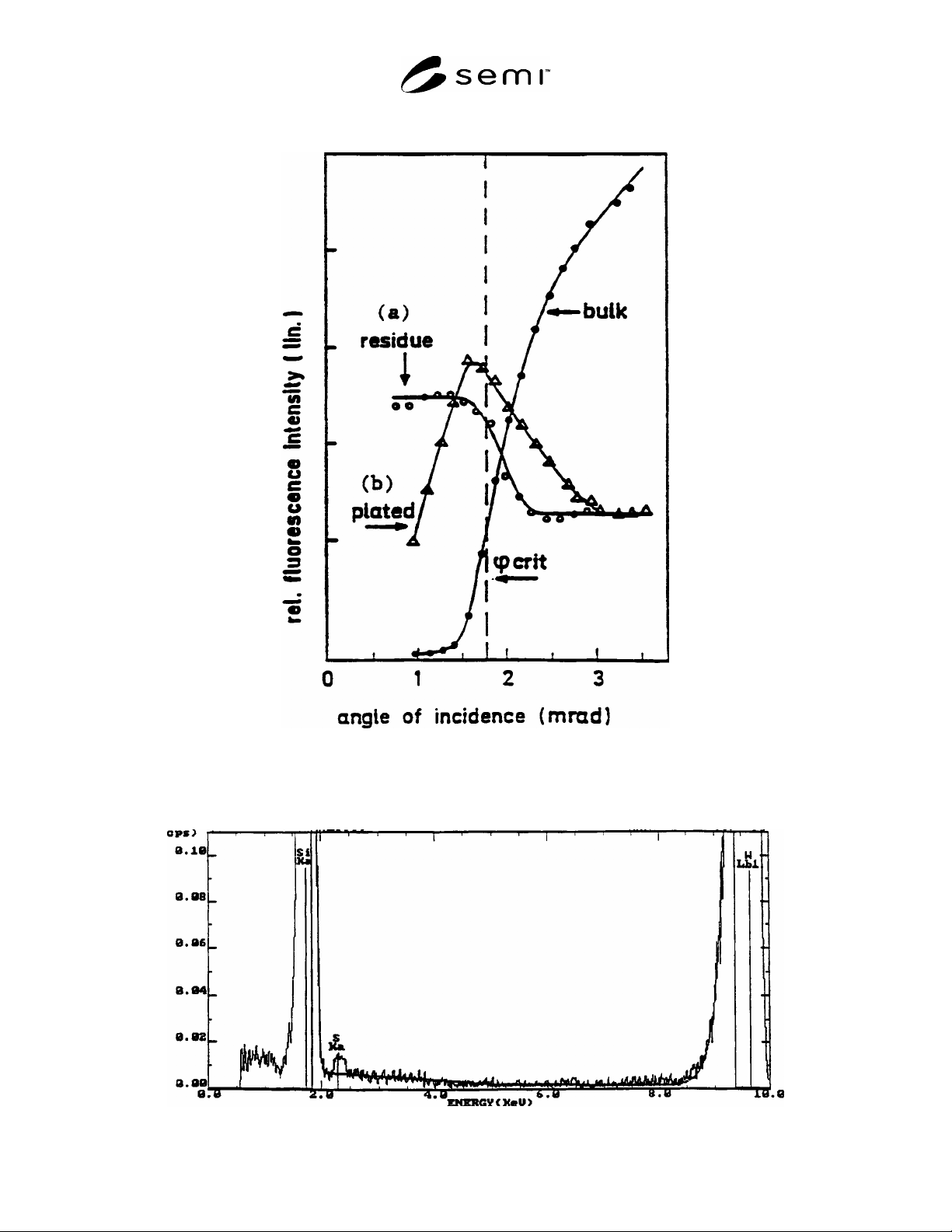
(1) A metal fluorescence count rate versus angle that is independent of glancing angle for angles 80 % below the critical angle (see Curve (a)
in Fig. 2
10
).
(2) A metal fluorescence count rate versus angle that is characteristic of metal contamination localized within a 3-nm thickness of the surface
(see Curve (b) in Fig. 2).
11.2 An anglescan of the calibration standard must be made to verify if the anglescan of the calibration element is similar to
Curve (a) (residue) or Curve (b) (in the film) in Fig. 2.
11.3 An appropriate non-TXRF measurement of the calibration standard must be agreed upon between parties in order to
assign the elemental areal density to the calibration standard element.
11.4 The calibration of the other elements detectable by the TXRF instrument must be completed using relative sensitivity
factor (RSFs) developed by the instrument manufacturer and stored in the instrument computer program. These RSFs are a
function of the X-ray source energy, the atomic number of the fluorescing element, and the fluorescence energy level, so if the
X-ray source energy is changed, a different set of RSFs must be used.
12. Procedure
12.1 Turn on the instrument in accordance with the manufacturer's instructions.
12.2 Analytical Conditions:
12.2.1 Choose and record the analytical conditions for the test specimen measurement. This includes:
12.2.1.1 Voltage to the X-ray source,
12.2.1.2 Current to the X-ray source,
12.2.1.3 Ambient in the analysis chamber,
12.2.1.4 Glancing angle,
12.2.1.5 Integration time,
12.2.1.6 X-ray source energy, and
12.2.1.7 Analysis location on the test specimen.
13. Calibration
13.1 Load the calibration specimen into the TXRF instrument in a contamination free environment defined by Class 100 or
better.
13.2 Measure the TXRF spectrum of the calibration specimen under the same operating conditions of current and voltage
applied to the X-ray source and of glancing angle to be used for the measurement of the test specimen. The measurement time
and the ambient (for example, vacuum, air, nitrogen, helium, etc) in the analysis chamber may be different between the
calibration and test specimen measurements. If the calibration anglescan is similar to Curve (b) of Fig. 2, use a glancing angle
which is 70 to 80 % of the critical angle. If the calibration anglescan is similar to Curve (a) of Fig. 2, use any glancing angle
that is below 85 % of the critical angle.
13.3 A polished silicon substrate with no detectable elemental contamination (that is, a BLANK), or a series of polished
silicon substrates each of which shows no detectable metal contamination for a selected element of interest (that is, a set of
element-specific BLANKs) and which collectively represent a blank for all elements of interest, must be measured by the
TXRF measurement under the condition of the test specimen to verify three are no instrumental background signals. An
example BLANK for all elements except sulfur is shown in Fig. 3.
13.4 Have the TXRF instrument integrate the calibration elemental fluorescence signal and subtract the background to
obtain a net integrated counts/second that corresponds to the assigned elemental areal density. The background may be
subtracted by a deconvolution routine or by a linear fit routine.
14. Report
14.1 Record the following information (see also 12.2.1):
14.1.1 Test specimen identification,
14.1.2 Calibration specimen identification,
10 Eichinger, P., Rath, H. J., and Schwenke, H., “Application of Total Reflection X-Ray Fluorescence Analysis for Metallic Trace Impurities on Silicon
Wafer Surfaces,” Semiconductor Fabrication: Technology and Metrology, ASTM STP 990, ASTM, 1989, pp. 305–313.
SEMI MF1526-95 © SEMI 2004 6
14.1.3 Anode material,
14.1.4 Monochromator,
14.1.5 Operator,
14.1.6 Date,
14.1.7 Type of instrument including model and manufacturer,
14.1.8 Software version,
14.1.9 Analysis time, and
14.1.10 Crystal orientation of the test specimen with respect to the incoming X-ray beam.
15. Precision and Bias
11
,
12
15.1 Precision—The precision was estimated through two round robins using monochromatic TXRF instruments.
15.1.1 The within-laboratory precision was estimated from a sequential round robin
12
that used two reference samples and
six unknowns with surface contamination of iron, nickel, copper and zinc, between 10
11
and 10
12
atoms/cm
2
. Thirteen
laboratories participated. At each laboratory the samples were measured once per day for 4 days. The measurement conditions
were X-ray rotating anode with a tungsten target, LiF (200) monochromator (9.67 keV line selected), 30 kV, 200 mA,
glancing angle of 0.05°, 10
2
torr ambient, 10-mm diameter analysis area, and 1000-s integration time. The data were reported
by each laboratory as the average of the four readings and the one standard deviation of the four readings. The 95 %
confidence, within-laboratory relative precision was 28 %, that is, 2.8 times the within-laboratory relative one standard
deviation of 10 %.
15.1.2 The between-laboratory precision was estimated from a spoke wheel round robin
13
that used sets of one reference
sample and three unknowns, one of which was a BLANK. The reference sample and the unknowns were contaminated with
surface nickel between 10
11
and 10
12
atoms/cm
2
. Seventeen organizations participated. At each laboratory the samples were
measured on multiple days. The measurement conditions were X-ray rotating anode with a tungsten or gold target,
monochromator (9.67 keV or higher line selected), 30 kV, 200 mA or higher, glancing angle of 0.1°, 10-mm diameter analysis
area, and 1000-s integration time. The 95 % confidence between-laboratory precision was: ±8 × 10
10
atoms/cm
2
at an
average 15 × 10
10
atoms/cm
2
, and ±20 × 10
10
atoms/ cm
2
at an average 45 × 10
10
atoms/cm
2
.
15.1.3 Analysis conditions other than those used for these round robins listed in 15.1.1 and 15.1.2 can be used, but the
precision has not been estimated for other analysis conditions.
15.2 Bias—The bias of this test method cannot be estimated, because there are no absolute standards for this test method.
16. Keywords
16.1 contamination; metals; silicone; surface; TXRF; X-ray fluorescence
11 Hockett, R. S., Ikeda, S., and Taniguchi, T., “TXRF Round Robin Results,” Cleaning Technology in Semiconductor Device Manufacturing, ECS
Proceedings, edited by J. Ruzyllo and R. E. Novak, Vol 92-12, The Electrochemical Society, Pennington, NJ, 1992, pp. 324–337.
12 Supporting data are available from ASTM Headquarters. Request RR: F01-1009 and F01-1012.
SEMI MF1526-95 © SEMI 2004 7
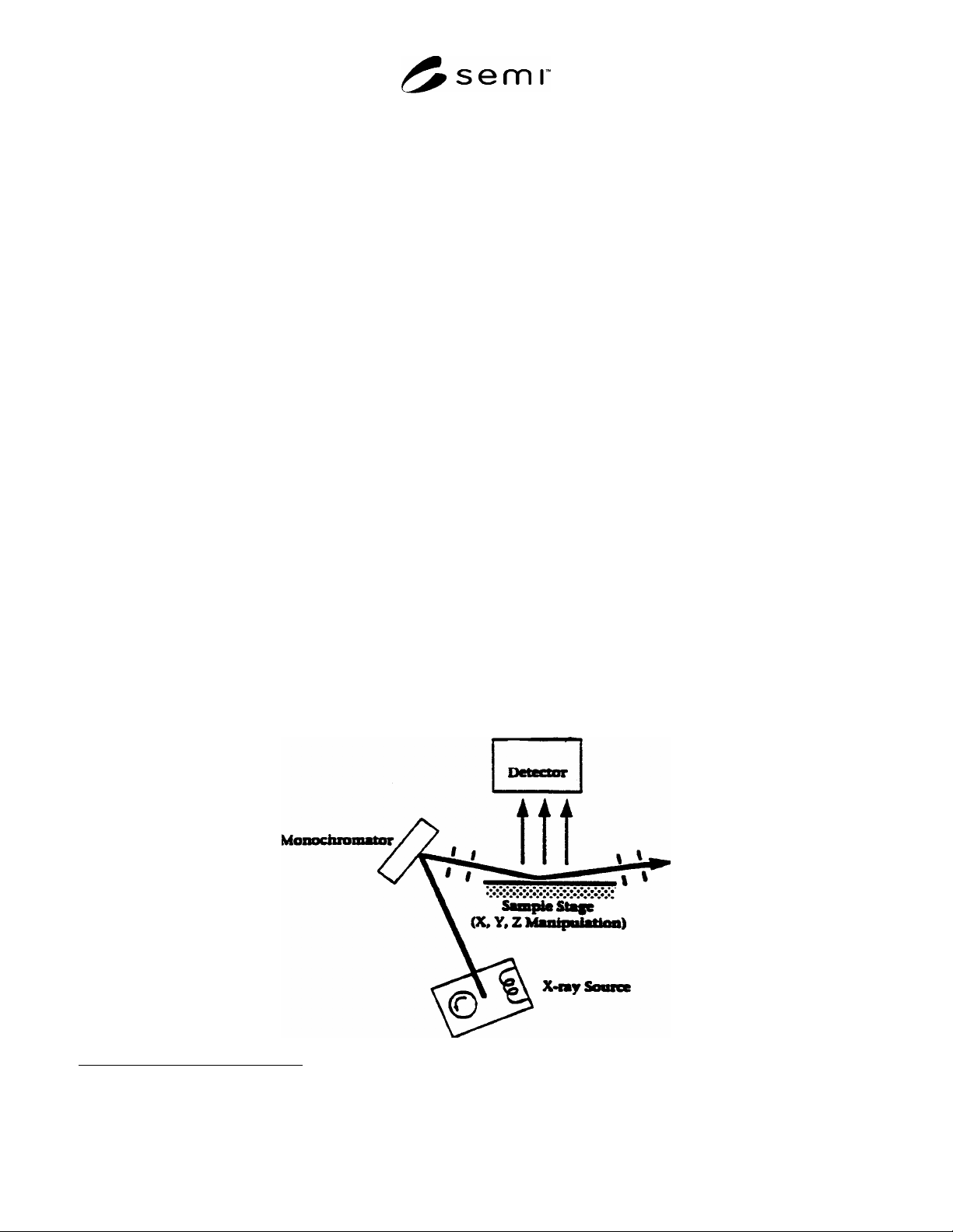
FIG. 1 Block Diagram of the TXRF Technique
FIG. 2 Experimental Curves for the Angular Dependence of the Fluorescence Intensity from Plated or Sputtered
Submonoatomic Nickel-layers (), Layers Produced by Evaporation of a Nickel Salt Solution (O) and the Silicon
Substrate (·)