semi合集-English.pdf - 第7440页
f ( x,y ) over the sp ecified r ange of x and y , and f ( x , y ) min = smal lest (most negative ) algebraic value of f ( x,y ) over the specified ra nge of x and y . In this case, use of eith er the focal plane or the r…

(in pairs) at intervals along the scan pattern. At each
measurement location, the sum of the displacements is
subtracted from D, yielding the thickness at each
measurement location as follows:
(2)
)],(),([),(),( yxbyxayxDyxt
where:
D = distance between Probes A and B,
a = distance between Probe A and the nearest
wafer surface,
b = distance between Probe B and the nearest
wafer surface, and
t = wafer thickness (see Figure 1).
13.2.2 Take the wafer thickness as the thickness at the
center point of the wafer.
13.2.3 Determine the total thickness variation, TTV, as
the largest thickness value, t
max
minus the smallest
thickness value, t
min
:
(3)
minmax
ttTTV
13.3 Flatness Determination
13.3.1 Construct the reference plane from the data set
t(x,y). The reference plane is of the following form (see
Notes 2 and 3):
(4)
RRRref
cybxaZ
where a
R
, b
R
, and c
R
are constants chosen as follows:
13.3.1.1 For ideal back surface reference plane,
(5) 0
RRR
cba
13.3.1.2 For the least squares reference plane, select
a
R
, b
R
, and c
R
so that (see Note 4):
(6)
yx
RRR
cybxayxt
,
2
)](),([
is minimized over the FQA for global determination,
over the portion of the site within the FQA for site
determination, or over the portion of the sub-site within
the FQA for sub-site determination.
13.3.1.3 For the three-point reference plane, construct
a plane so that
(7)
RRR
RRR
RRR
cybxayxt
cybxayxt
cybxayxt
3333
2222
1111
),(
and,),(
,),(
where x
1
, y
1
; x
2
y
2
; and x
3
, y
3
are equally spaced points
located on a circle whose perimeter is located 3 mm
from the edge of a wafer of nominal diameter (see Note
4).
13.3.2 Construct a focal plane to calculate deviation
parameters from the data set t(x,y). The focal plane is
of the following form:
FFFfocal
cybxaZ
(8)
The focal plane is parallel with the reference plane so
that in all cases
a
F
= a
R
, and
b
F
= b
R
.
13.3.2.1 A global focal plane is the same as the
corresponding reference plane so that
c
F
= c
R
.
13.3.2.2 A site or sub-site focal plane is displaced from
the corresponding reference plane as follows:
c
F
= t(x
0
,y
0
) (a
F
x
0
+ b
F
y
0
)
where x
0
and y
0
are the coordinates of the site or sub-
site center, respectively.
NOTE 2: Use of the thickness data set, t(x,y), in this regard is
equivalent to setting the origin of the z-axis, as defined in
SEMI M20, at the back surface of the wafer at each point of
the data set. Then the value of z at each point is equal to the
thickness t at that point. This is equivalent to constraining the
wafer so that the back surface is pulled down uniformly onto
an ideal chuck.
NOTE 3: The constants a
R
and a
F
provide the slopes of the
reference and focal planes, respectively, in the x direction, the
constants b
R
and b
F
provide the slopes of the reference and
focal planes, respectively, in the y direction, and the constants
c
R
and c
F
provide the distances of the center point of the
reference and focal planes, respectively, from the back surface
at that point.
NOTE 4: The values t(x,y) at any point represent z
f
(x,y),
where z
f
is the height of the front surface from the z-axis
origin at each point. It is use of this data set that causes the
reference surface to be the front surface for both the least
squares and three-point reference planes.
13.3.3 Determine the point-by-point differences
between the thickness and the reference or focal plane
by
)(),(),(
iii
cxbxayxtyxf
(9)
where the subscript i is either R or F depending on
whether a reference or focal plane is being used and x
and y range over the FQA, the site, or the sub-site, for
global, site, or sub-site determinations.
13.3.4 Determine range (also called TIR) as follows:
minmax
),(),( yxfyxfTIR
(10)
where:
f
(x,y)
max
= largest (most positive) algebraic value of
SEMI MF1530-1104 © SEMI 2003, 2004 5
f
(x,y) over the specified range of x and y,
and
f
(x,y)
min
= smallest (most negative) algebraic value
of f(x,y) over the specified range of x
and y.
In this case, use of either the focal plane or the
reference plane results in the same answer.
NOTE 5: GBIR, the flatness TIR with an ideal global back
surface reference plane, is equal to the TTV. However, TTV
can be obtained from the t(x,y) data set without construction
of the reference plane.
13.3.5 Determine focal plane deviation (FPD) using
the focal plane. The FPD is given by the larger of
|f(x,y)
max
| or |f(x,y)
min
|.
13.3.6 Record the determined values.
13.3.7 For referee or other measurements where the
wafer is measured more than once, calculate the
maximum, minimum, sample standard deviation,
average and range of all measurements on each wafer
measured.
13.3.7.1 Record sample standard deviation and other
statistical parameters as agreed upon between the
parties to the test.
14 Report
14.1 Report the following information:
14.1.1 Date, time, and temperature of test,
14.1.2 Identification of operator,
14.1.3 Location (laboratory) of test,
14.1.4 Identification of measuring instruments,
including wafer-holding device diameter, data point
spacing, sensor size, and measurement method,
14.1.5 Lot identification, including nominal diameter,
nominal center-point thickness, and nominal edge
exclusion (EE) specified.
14.1.6 Description of sampling plan, and one or more
of the following parameters as required by the
application:
14.1.7 Center-point thickness of each wafer measured,
14.1.8 Total thickness variation of each wafer
measured, and
14.1.9 Flatness parameter of each wafer measured, and
described as one or more of the following choices:
14.1.9.1 The global flatness, or
14.1.9.2 The maximum value of site flatness as
measured on all sites, or
14.1.9.3 The percentage of sites which have a site
flatness less than or equal to a specified value, or
14.1.9.4 The individual flatness value of each site.
14.2 For referee tests the report shall also include the
standard deviation of each set of wafer measurements
and, if required, the flatness distribution of all sites on
all wafers measured, when site flatness is measured.
15 Precision and Bias
15.1 Twenty-three 200 mm diameter, single-side
polished silicon wafers were employed in a round-robin
experiment. These wafers represented three different
manufacturing processes. All three subsets were bare
on the front surface. Two subsets were bare on the
back surface and one subset had oxide on the back
surface.
15.2 Eight laboratories measured thickness. Six of
these laboratories also measured flatness. Each of the
twenty-three wafers was measured three times in
succession (in three cassette-to-cassette “passes”), on a
single day on automatic measurement systems, in
accordance with this test method.
15.3 All measurement data were acquired with 3 mm
nominal edge exclusion.
15.4 Flatness values were calculated in an array of 15
by 15 mm sites, and a 7.5 mm array offset in both
x and
y directions, relative to the wafer center. Within this
137-site array, precision statistics were derived for four
selected sites, two “full” sites in the central area and
two “partial” sites along the FQA boundary, as
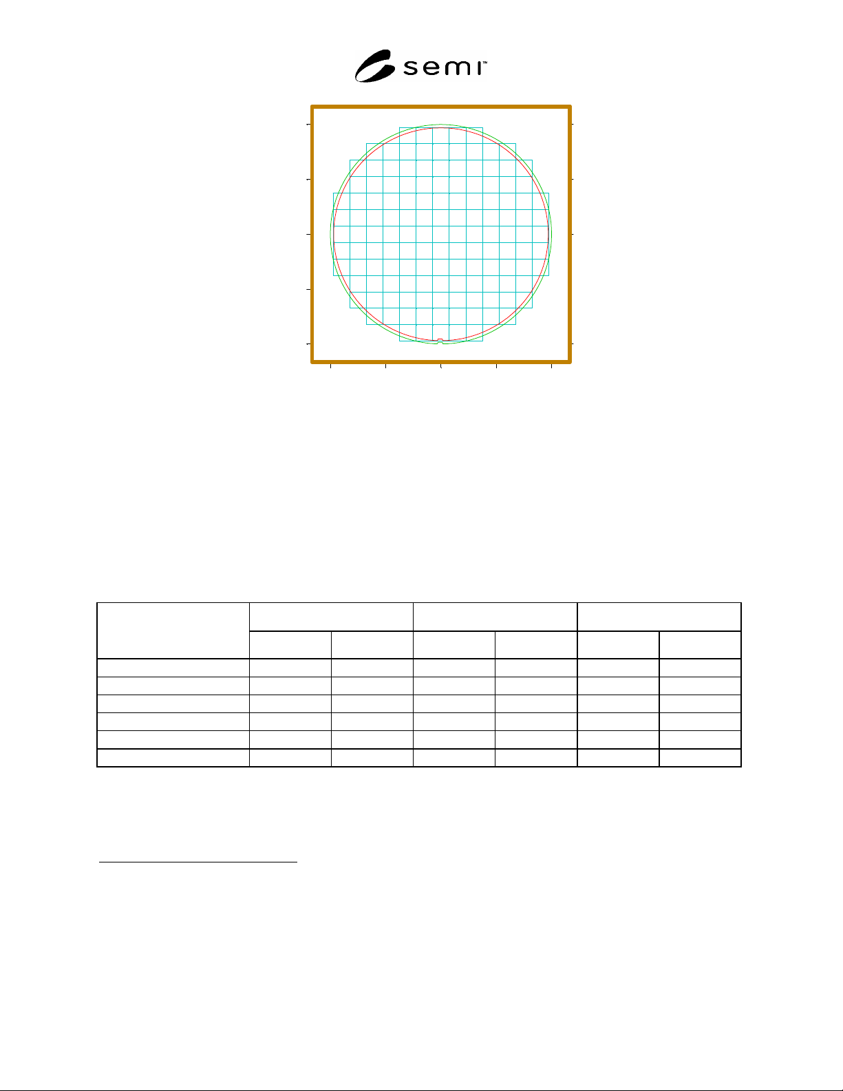
indicated in Table 2. Figure 2 shows these sites within
the complete 137-site array.
Table 2 Site Information
Site ID Site Type Location on Wafer
69 Full Center
73 Full 60 mm from Center (0°)
75 Partial FQA Boundary (0°)
135 Partial Notch (270°)
15.5 The number of laboratories, samples, and
determinations in this study met the minimum
requirements for determining precision prescribed in
ASTM Practice E 691.
15.6 The ranges of 95% confidence interval, within
which two measurements are considered statistically to
be the same, for within-laboratory repeatability (r) and
between-laboratory reproducibility (R) are shown in
Table 3.
SEMI MF1530-1104 © SEMI 2003, 2004 6
X
Y
-100 -50 0 50 100
-100
-50
0
50
100
1 2 3 4 5
6 7 8 9 10 11 12 13 14
15 16 17 18 19 20 21 22 23 24 25
26 27 28 29 30 31 32 33 34 35 36
37 38 39 40 41 42 43 44 45 46 47 48 49
50 51 52 53 54 55 56 57 58 59 60 61 62
63 64 65 66 67 68 69 70 71 72 73 74 75
76 77 78 79 80 81 82 83 84 85 86 87 88
89 90 91 92 93 94 95 96 97 98 99 100 101
102 103 104 105 106 107 108 109 110 111 112
113 114 115 116 117 118 119 120 121 122 123
124 125 126 127 128 129 130 131 132
133 134 135 136 137
Wed Jun 30 09:30:04 1999
siteX = 15 siteY = 15 Diam = 200 Edge Excl. = 3 X-off = 0 Y-off = 0
Figure 2
15 mm by 15 mm Site Array on 200 mm Wafer with 3 mm Nominal Edge Exclusion
15.7 Figures 3 through 8 contain plots of repeatability (r) and reproducibility (R) for the various parameters: center-
point thickness and TTV for the wafers, and SBIR for the four analyzed sites against mean value.
15.8 For more details, refer to the Research Report.
2
16 Keywords
flatness; noncontact measurement; semiconductor; silicon; thickness; thickness variation; wafers
Table 3 Summary Measurement Statistics
Mean,
m r,
m R,
m
Parameter
Smallest Largest Smallest Largest Smallest Largest
Center Point Thickness 714.86 735.87 0.028 0.085 0.563 1.039
TTV 0.94 2.39 0.026 0.091 0.100 0.292
SBIR Site 069 0.09 0.24 0.010 0.012 0.017 0.095
SBIR Site 073 0.14 0.54 0.013 0.026 0.015 0.037
SBIR Site 075 0.29 1.16 0.017 0.093 0.109 0.243
SBIR Site 135 0.20 1.05 0.015 0.068 0.035 0.892
2 Available on request from SEMI Headquarters, Publications Department, 3081 Zanker Road, San Jose, CA, Fax: 408-943-7015. Request
International Standards Research Report F01–1016, ASTM Interlaboratory Round Robin Experiment on Measuring Warp on Silicon Wafers by
Automated Noncontact Scanning and Measuring Flatness, Thickness and Thickness Variation of Silicon Wafers by Automated Noncontact
Scanning.
SEMI MF1530-1104 © SEMI 2003, 2004 7