semi合集-English.pdf - 第7690页
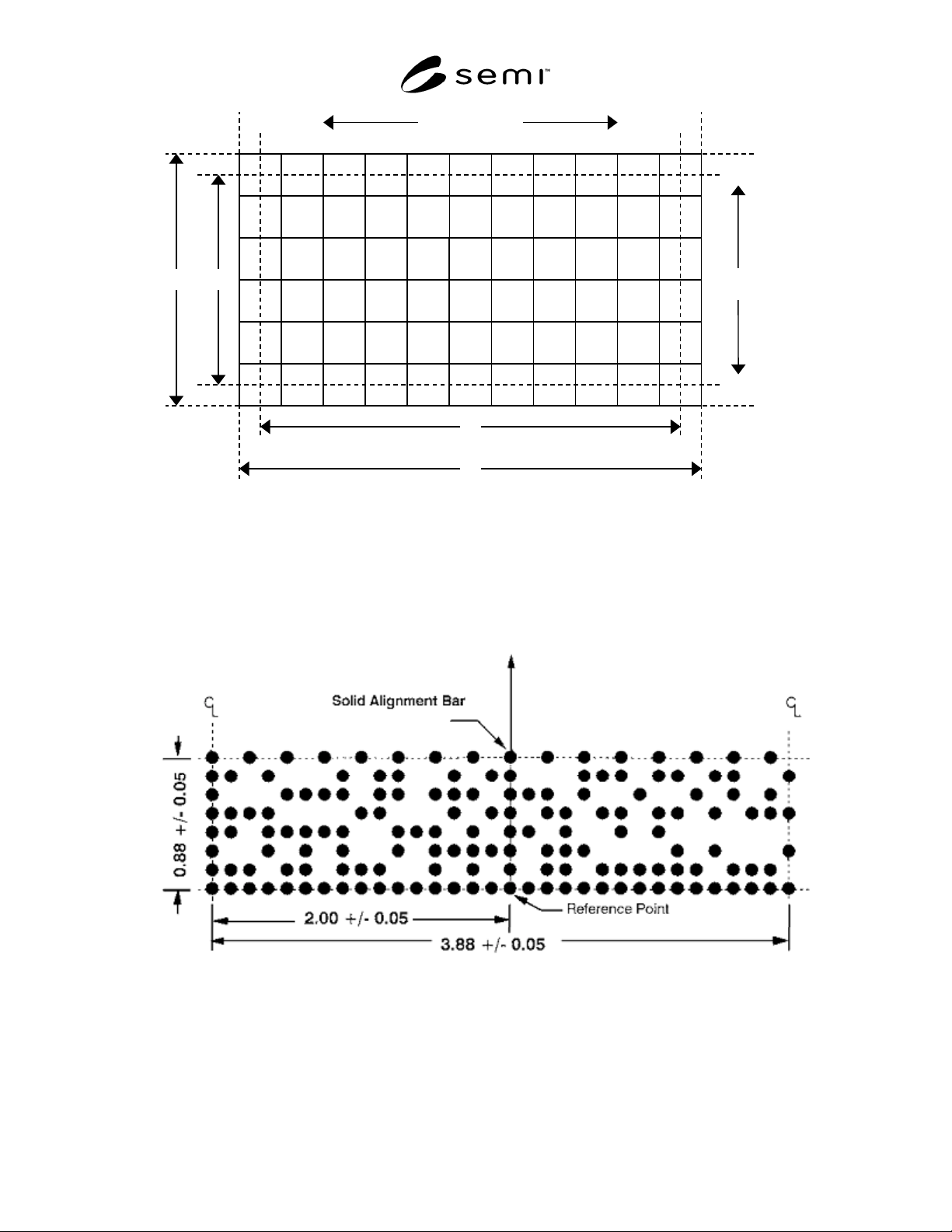
SEMI T7-0303 © SEMI 1997, 2003 3 32 cells per row C1 C2 R1 R2 8 cells per column Nominal Di mensions ( mm) R1 = 3.875 C1 = 0.875 R2 = 4.000 C2 = 1.000 C L C L C L C L Figure 2 Data Matrix Field Dimensions ECC200 - 8 rows…
SEMI T7-0303 © SEMI 1997, 2003 2
4.1.10 data matrix code symbol — a two-dimensional
array of square cells arranged in contiguous rows and
columns. In certain ECC200 symbols, data regions are
separated by alignment patterns. The data region is
surrounded by a finder pattern [ISO/IEC 16022].
4.1.11 dot — a localized region with a reflectance
which differs from that of the surrounding surface.
NOTE 1: To assure reading efficiency, a minimum contrast
of 30% is required between the reflectance value of a dot and
the surrounding wafer surface. Various densitometers can
provide such measurements nondestructively.
4.1.12 dot misalignment, within a cell — the distance
between the physical center point of a dot and the cell
center point.
4.1.13 finder pattern, of a data matrix code symbol —
a perimeter to the data region. Two adjacent sides
contain dots in every cell; these are used primarily to
define physical size, orientation and symbol distortion.
The two opposite sides are made up of cells containing
dots in alternate cells [ISO/IEC 16022].
4.1.14 reference point, of a data matrix code symbol —
the physical center point of a corner cell common to the
primary border row and the solid line of the alignment
bar, used to identify the physical location of the symbol
on the object being marked with the symbol.
NOTE 2: The reference point is at a fixed location on the
object. Different cells may be chosen as the reference point
depending on the desired orientation of the symbol on the
object and the size variability of the symbol. The particular
cell to be used as the reference point must be specified for
each application.
5 Requirements
5.1 Shape and Size of the Data Matrix Code Symbol
5.1.1 Data Matrix Code Symbol Dimensions
5.1.1.1 Each rectangular matrix code symbol shall be
composed of an array of 8 rows and 32 columns with an
alignment bar as defined in ISO/IEC ISS 16022.
5.1.1.2 Cell spacing shall be 125 µ m, center to center.
5.1.2 Dot Size — The nominal shape of the dot
produced in the matrix may be circular or square. Its
diameter or edge length (after polishing) shall be 100
µ m + 10 µ m – 20 µ m.
5.1.3 Border Rows and Columns
5.1.3.1 One border row and one border column shall
contain a dot in each cell. These are identified as the
primary border row and the primary border column.
These are used by the code reader to determine the
orientation of the matrix.
5.1.3.2 The opposing (secondary) border row and
column shall contain dots in alternating cells.
5.1.3.3 For these rectangular matrix code symbols, the
reference point of the symbol shall be the physical
centerpoint of the cell common to the primary border
row and the center alignment bar.
5.1.4 The maximum dot misalignment within a cell is
15 µ m. This ensures that a minimum size dot covers a
cell central area of radius 25 µ m.
5.1.5 Adjacent dots shall not touch.
5.2 Content of the Data Matrix Code Symbol
5.2.1 Each rectangular matrix code symbol shall
contain 10 message characters, together with the error
checking and correcting (ECC200) code characters,
encoded in accordance with ISO/IEC ISS 16022.
5.2.2 The message characters may include the
following: A–Z, 0–9, and dash (–). These characters
constitute the SEMI OCR Character Set except for the
period (.); this is the same character set specified in
SEMI M12. These characters are also included in the
set designated as “primarily upper case alphanumeric”
in ISO/IEC 16022, in Table 5 and Annexe J. The ten
message characters shall contain two elements:
a. a vendor-assigned 8-character wafer identification
code, followed by
b. a 2-character vendor identification code (see SEMI
AUX001).
5.3 Location of the Data Matrix Code Symbol
5.3.1 With the wafer positioned back surface up and
with the primary fiducial (notch) toward the operator,
the origin of the data matrix code symbol shall be
located as specified below.
5.3.1.1 The 8 row × 32 column rectangular 2-D matrix
code symbol shall be placed entirely outside a fixed
quality area (FQA) with a nominal edge exclusion of 3
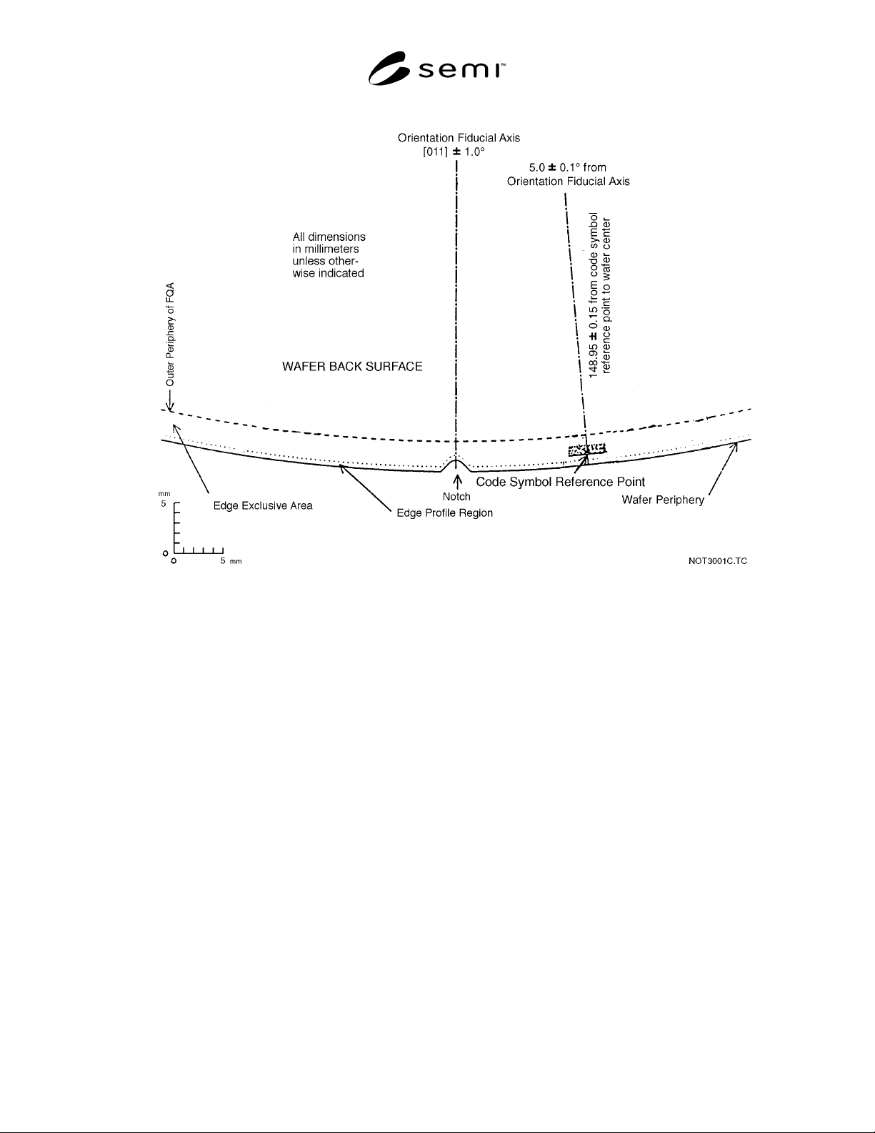
mm. The reference point shall be located 148.95 ± 0.15
mm from the center of the wafer, along a radius 5.0 ±
0.1° counterclockwise from the axis of the notch
fiducial bisector.
5.3.2 The primary row of the matrix code symbol shall
be placed toward the periphery of the wafer.
SEMI T7-0303 © SEMI 1997, 2003 3
32 cells per row
C1 C2
R1
R2
8 cells per
column
Nominal Dimensions (mm)
R1 = 3.875
C1 = 0.875
R2 = 4.000
C2 = 1.000
C
L
C
L
C
L
C
L
Figure 2
Data Matrix Field Dimensions
ECC200 - 8 rows × 32 columns
To Wafer Cente
r
Dimensions in millimeters are o
f
center to center of dots
Figure 3
Data Matrix Code Fields
ECC200 - 8 rows × 32 columns
SEMI T7-0303 © SEMI 1997, 2003 4
Figure 4
Data Matrix Code Symbol Location on Back Surface of Notched 300 mm Diameter Wafer
NOTE 1: The peripheries are of wafers of nominal diameter with nominal notch dimensions. The dots of the finder pattern are
shown for an 8 row x 32 column data matrix code symbol with 125 µ m spacing.
NOTICE: These standards do not purport to address safety issues, if any, associated with their use. It is the
responsibility of the user of these standards to establish appropriate safety and health practices and determine the
applicability of regulatory limitations prior to use. SEMI makes no warranties or representations as to the suitability
of the standards set forth herein for any particular application. The determination of the suitability of the standard is
solely the responsibility of the user. Users are cautioned to refer to manufacturer’s instructions, product labels,
product data sheets, and other relevant literature respecting any materials mentioned herein. These standards are
subject to change without notice.
The user’s attention is called to the possibility that compliance with this standard may require the use of copyrighted
material or of an invention covered by patent rights. RVSI Acuity CiMatrix has filed a statement with SEMI
asserting that the patented or copyrighted item can be used by the public for the purpose of implementing this
standard without specific license and without payment of royalty or other charge. Attention is also drawn to the
possibility that some elements of this standard may be subject to patented technology or copyrighted items other
than those identified above. Semiconductor Equipment and Materials International (SEMI) shall not be held
responsible for identifying any or all such patented technology or copyrighted items. By publication of this
standard, SEMI takes no position respecting the validity of any patent rights or copyrights asserted in connection
with any item mentioned in this standard. Users of this standard are expressly advised that determination of any
such patent rights or copyrights and the risk of infringement of such rights are entirely their own responsibility.
Copyright by SEMI® (Semiconductor Equipment and Materials
International), 3081 Zanker Road, San Jose, CA 95134. Reproduction o
f
the contents in whole or in part is forbidden without express written
consent of SEMI.