semi合集-English.pdf - 第5368页
SEMI M55-0705 © SEMI 2003, 2004 2 SEMI M12 Specification for Serial Alphanum eric Ma rking of the Front Surface of Wafers 3.2 ASTM Standar d s 2 ASTM E122 Standard Practice for Calc ulating Sample Size to Estimate, W…
SEMI M55-0705 © SEMI 2003, 2004 1
SEMI M55-0705
SPECIFICATION FOR POLISHED MONOCRYSTALLINE SILICON
CARBIDE WAFERS
This specification was technically approved by the Global Compound Semiconductor Committee and is the
direct responsibility of the European Compound Semiconductor Materials Committee. Current edition
approved by the European Regional Standards Committee on January 8, 2003. Initially available at
www.semi.org January 2003; to be published March 2003.
NOTICE: The designation of SEMI M55 was updated during the 0705 publishing cycle to reflect the
creation of SEMI M55.2.
1 Purpose
1.1 These specifications cover substrate requirements for monocrystalline high-purity silicon carbide wafers of
crystallographic polytype 6H and 4H used in semiconductor and electronic device manufacturing.
2 Scope
2.1 A complete purchase specification may require that additional physical, electrical, and bulk properties be
defined. These properties are listed, together with test methods suitable for determining their magnitude where such
procedures are documented.
2.2 These specifications are directed specifically to silicon carbide wafers with one or both sides polished.
Unpolished wafers or wafers with epitaxial films are not covered; however, purchasers of such wafers may find
these specifications helpful in defining their requirements.
2.3 The material is Single Crystal Silicon Carbide (SiC) existing in many crystallographically different polytypes.
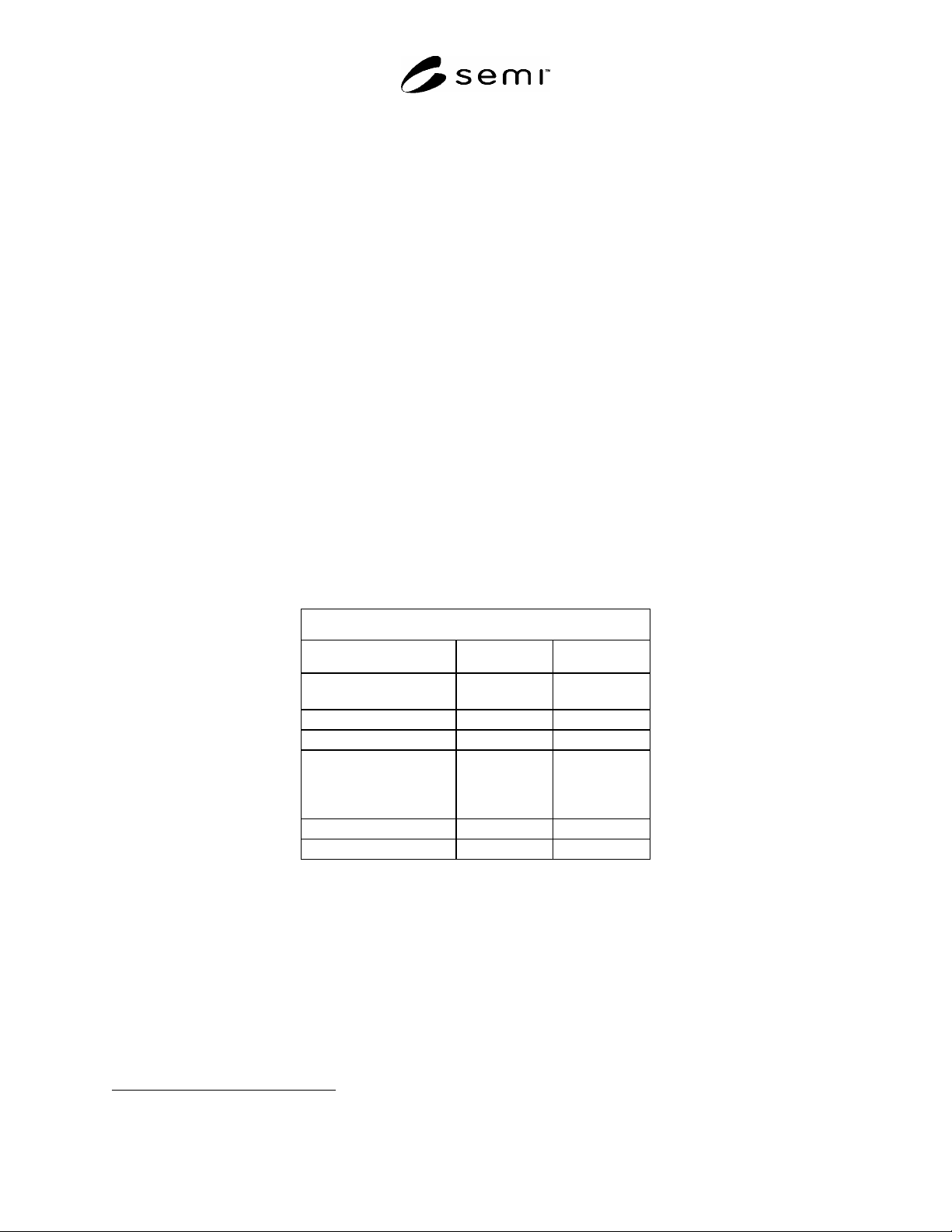
For the most common polytypes the following properties in Table 1 are listed for use as guidelines:
Table 1 Common Properties
1
Polytype 4H
6H
Lattice Parameter a
c
3.076 Å
10.053 Å
3.073 Å
15.117 Å
Stacking Sequence ABAC ABCACB
Density 3.21 g/cm
3
3.21 g/cm
3
Melting Point chemical
decomposition
above ca.
2800°C
chemical
decomposition
above ca.
2800°C
Dielectric Constant 9.7 9.7
Energy Gap 3.27 eV 3.02 eV
2.4 For referee purposes, SI (System International, commonly called metric) units shall be used.
NOTICE: This standard does not purport to address safety issues, if any, associated with its use. It is the
responsibility of the users of this standard to establish appropriate safety and health practices and determine the
applicability of regulatory or other limitations prior to use.
3 Referenced Standards
3.1 SEMI Standards
SEMI M1 Specification for Polished Mono-crystalline Silicon Wafers
1 Data as reported in Landolt-Börnstein (Springer Verlag)

SEMI M55-0705 © SEMI 2003, 2004 2
SEMI M12 Specification for Serial Alphanumeric Marking of the Front Surface of Wafers
3.2 ASTM Standards
2
ASTM E122 Standard Practice for Calculating Sample Size to Estimate, With a Specified Tolerable Error, the
Average for Characteristic of a Lot or Process
ASTM F26 Standard Test Methods for Determining the Orientation of a Semiconductive Single Crystal
ASTM F154 Standard Guide for Identification of Structures and Contaminants Seen on Specular Silicon Surfaces
ASTM F523 Standard Practice for Unaided Visual Inspection of Polished Silicon Wafer Surfaces
ASTM F533 Standard Test Method for Thickness and Thickness Variation of Silicon Wafers
ASTM F534 Standard Test Method for Bow of Silicon Wafers
ASTM F657 Standard Test Method for Measuring Warp and Total Thickness Variation on Silicon Wafers by
Noncontact Scanning
ASTM F671 Standard Test Method for Measuring Flat Length on Wafers of Silicon and Other Electronic
Materials
ASTM F673 — Standard Test Methods for Measuring Resistivity of Semiconductor Slices or Sheet Resistance of
Semiconductor Films with a Noncontact Eddy-Current Gage
ASTM F847 — Standard Test Methods for Measuring Crystallographic Orientation of Flats on Single Crystal
Silicon and Wafers by X-Ray Techniques
ASTM F928 Standard Test Methods for Edge Contour of Circular Semiconductor Wafers and Rigid Disk
Substrates
ASTM F1390 — Standard Test Method for Measuring Warp on Silicon Wafers by Automated Noncontact Scanning
ASTM F1404 — Test Method for Crystallographic Perfection of Gallium Arsenide by Molten Potassium Hydroxide
(KOH) Etch Technique
ASTM F1530 — Standard Test Method for Measuring Flatness, Thickness, and Thickness Variation on Silicon
Wafers by Automated Noncontact Scanning
ASTM F2074 — Standard Guide for Measuring Diameter of Silicon and Other Semiconductor Wafers
3.3 DIN Standards
3
DIN 50441/1 — Measurement of the Geometric Dimensions of Semiconductor Wafers: Thickness and Thickness
Variation
DIN 50448 — Testing of materials for semiconductor technology - Contactless determination of the electrical
resistivity of semi-insulating semiconductor slices using a capacitive probe
3.4 JIS Standard
4
JIS H 0611 — Methods of Measurement of Thickness Taper and Bow for Silicon Wafers
3.5 Other Standards
ANSI/ASQC Z1.4 — Sampling Procedures and Tables for Inspection by Attributes
5
NOTICE: Unless otherwise indicated, all documents cited shall be the latest published versions.
2 American Society for Testing and Materials, 100 Barr Harbor Drive, West Conshohocken, Pennsylvania 19428-2959, USA. Telephone:
610.832.9585, Fax: 610.832.9555 Website: www.astm.org
3 Available from Deutches Institut für Normung e.V., Beuth Verlag GmbH, Burggrafenstrasse 4-10, D-10787 Berlin, Germany, website:
www.din.de
4 Japanese Industrial Standards, Available through the Japanese Standards Association, 1-24, Akasaka 4-Chome, Minato-ku, Tokyo 107-8440,
Japan. Telephone: 81.3.3583.8005; Fax: 81.3.3586.2014 Website: www.jsa.or.jp
5 American Society for Quality Control, 611 East Wisconsin Avenue, Milwaukee, WI 53202, USA

SEMI M55-0705 © SEMI 2003, 2004 3
4 Terminology
NOTE 1: Many definitions and terms not given in this section can be found in SEMI M1, the SEMI Compilation of Terms, and
ASTM F154.
4.1 Definitions
4.1.1 bow of a semiconductor wafer, a measure of concave or convex deformation of the median surface of a
wafer, independent of any thickness variation which may be present. Bow is a bulk property of the test specimen,
not a property of an exposed surface. Generally, bow is determined with a test specimen in a free, unclamped
condition. Units of bow are generally micrometers.
4.1.2 crystallite — any part of the wafer, having an arbitrary orientation of its crystallographic axis in respect to the
monocrystalline part of the wafer.
4.1.3 dopant a chemical element, usually from the third or fifth column of the periodic table for the case of IV-
IV compounds, incorporated in trace amounts in a semiconductor crystal to establish its conductivity type and
resistivity.
4.1.4 edge contouring on wafers whose edges have been shaped by mechanical and/or chemical means, a
description of the profile of the boundary of the wafer joining the front and back sides.
4.1.5 edge exclusion the width X of a narrow band of wafer surface, located just inside the wafer edge, over
which the values of the specified parameter do not apply. See definition of fixed quality area below.
4.1.6 fixed quality area (FQA) — The central area of a wafer surface, defined by a nominal edge exclusion, X, over
which the specified values of a parameter apply.
4.1.6.1 Discussion — The boundary of the FQA is at all points the distance X away from the periphery of a wafer of
nominal dimensions. (See Figure 1.) The size of the FQA is independent of wafer diameter and flat length
tolerances.
4.1.7 lot for the purpose of this document, (a) all of the wafers of nominally identical size and characteristics
contained in a single shipment, or (b) subdivisions of large shipments consisting of wafers as above which have been
identified by the supplier as constituting a lot.
4.1.8 micropipe small hollow tube approximately parallel to the crystallographic c-axis and extending through
the whole crystal.
4.1.9 orthogonal misorientation in {0001} wafers cut intentionally “off-orientation”, the angle between the
projection of the vector normal to the wafer surface onto the {0001} plane and the projection on that plane of the
specified direction of tilt in the {0001} plane. (See Figure 2.)
4.1.10 planar defect
small cavity in a SiC bulk crystal with large width-to-height ratio roughly parallel to the
{0001} lattice plane. The lateral boundaries are parallel to crystallographic directions. Often one or more
micropipes are connected to a planar defect.
4.1.11 polytype one possible crystallographic modification of a substance which shows the phenomenon of
polytypism. All polytypes of a substance have the same lattice layers with nearly the same lattice constant in
common. However the stacking sequence of these layers differs between different polytypes. Most commonly
polytypes are named after a suggestion of Ramsdell
6
: A symbol like 6H gives the number of layers in one periodic
stacking sequence (2, 3, 4, ... ) and the symmetry of the resulting crystal (H = hexagonal, R = rhombohedral). The
most common polytypes of SiC are 6H, 4H, 15R.
4.1.12 surface orientation the tilt angle between the crystallographic c-axis and the wafer surface normal. (See
Figure 2.)
4.1.13 total indicator reading (TIR) — the smallest perpendicular distance between two planes, both parallel with
the reference plane, which encloses all points on the front surface of a wafer within the FQA, the site, or the subsite,
depending on which is specified.
6 L. S. Ramsdell, J. A. Kohn: Developments in Silicon Carbide Research, Acta Cryst. 5 (1952) 215 – 224