semi合集-English.pdf - 第7414页
SEMI MF1527-1104 © SEMI 2003, 2004 20 curve drawn t hrough the ex perimental data 18 by more than 0.0002 ( ·c m)/( ·cm·°C). SEMI MF84 includes a table of values calculated fro m this fit and extended down to 0. 0006 …
SEMI MF1527-1104 © SEMI 2003, 2004 19
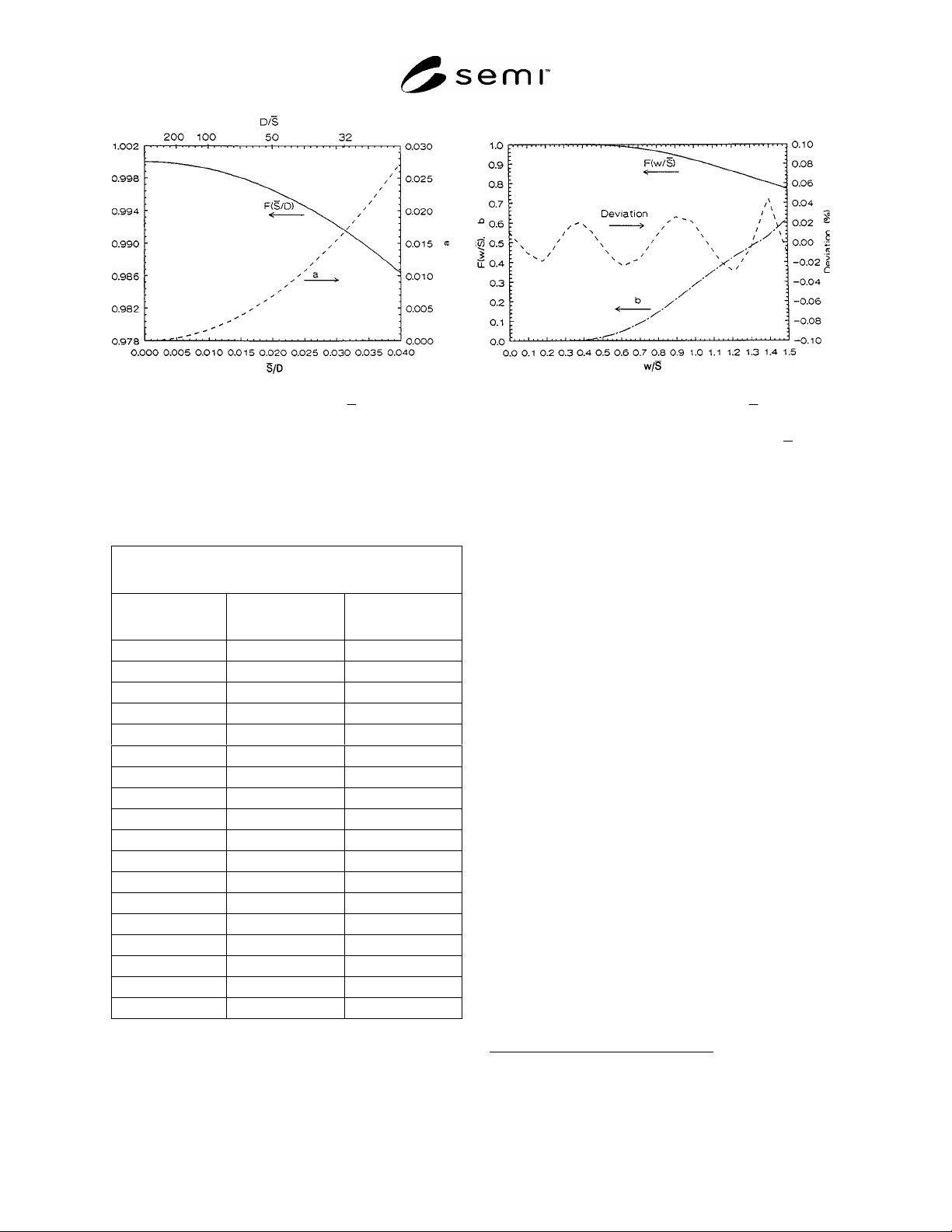
Figure R2-1 Figure R2-2
Diameter Correction Factor, F(
S /D), and Thickness Correction Factor, F(w/ S ), Error
Error Coefficient, a Coefficient, b, and Percentage Deviation
between Fit (Equation R2-7) and F(w/
S )
R2-3.3.2 Uncertainty in probe-tip spacing arises both
from the error in measurement and from probe-tip
wander.
R2-4 Temperature Correction Factor—SEMI MF84
requires that the resistivity of a silicon wafer be
corrected to its value at 23°C. Between 18° and 28°C,
the resistivity of silicon can be treated as a linear
function of the temperature; over this temperature
range, the temperature correction factor, F
T
is given as
follows:
)23(1
TCF
TT
(R2-12)
where:
C
T
= temperature coefficient of resistivity,
(·cm)/(·cm·°C), and
T = temperature, °C, at which the resistivity
measurement was made.
R2-4.1 The temperature coefficient has been deter-
mined experimentally as a function of the resistivity of
both boron- and phosphorus-doped silicon.
18
As
outlined in SEMI MF84, the experimental data have
been fitted with polynomials of the form:
k
n
n
nT
AC
0
)(ln
(R2-13)
where:
A
n
= the appropriate coefficients (see Table R2-1),
=
wafer resistivity, ·cm, and
k = 17 for phosphorus-doped silicon and 13 for boron-
doped silicon.
R2-4.2 These polynomials are such that nowhere
within the resistivity range 0.001 and 500 ·cm does
the value of C
T
derived from them deviate from the
18 Bullis, W. M., Brewer, F. H., Kolstad, C. D., and Swartzendruber,
L. J., “Temperature Coefficient of Resistivity of Silicon and
Germanium Near Room Temperature,” Solid-State Electron. 11, 639–
646 (1968).
Table R2-1 Polynominal Coefficients for
Temperature Coefficient of Resistivity, %/°C
Coefficient
Phosphorus-Doped
Silicon
Boron-Doped
Silicon
A
0
7.364 × 10
1
7.068 × 10
1
A
1
6.560 × 10
2
8.544 × 10
2
A
2
3.075 × 10
2
1.478 × 10
2
A
3
2.427 × 10
3
1.635 × 10
3
A
4
7.5883 × 10
3
2.003 × 10
3
A
5
7.5541 × 10
4
3.415 × 10
4
A
6
1.39760 × 10
3
2.0915 × 10
4
A
7
1.159 × 10
6
4.3237 × 10
5
A
8
1.106882 × 10
4
7.0532 × 10
6
A
9
4.56719 × 10
6
1.60868 × 10
6
A
10
4.407686 × 10
6
1.0346 × 10
7
A
11
2.601512 × 10
7
2.5201 × 10
8
A
12
9.408560 × 10
8
5.6419 × 10
10
A
13
6.190700 × 10
9
1.4445 × 10
10
A
14
1.032377 × 10
9
A
15
6.890181 × 10
11
A
16
4.58514 × 10
12
A
17
2.94332 × 10
13

SEMI MF1527-1104 © SEMI 2003, 2004 20
curve drawn through the experimental data
18
by more
than 0.0002 (·cm)/(·cm·°C). SEMI MF84 includes a
table of values calculated from this fit and extended
down to 0.0006 ·cm and up to 100 ·cm by taking
smoothed values to avoid the oscillations of the
polynomials in the extreme regions.
R2-5 By substituting these relations into Equation R2-
4, one obtains the following:
T
T
C
C
F
TC
I
I
V
V
S
S
S
S
ba
w
w
b
D
D
a
d
dd
d
082.1
d
)082.1(
d
)1(
d
d
2
2
23
23
(R2-14)
R2-6 Estimates of the errors in resistivity measurement
due to uncertainties in diameter, thickness and probe-tip
spacing can be made by inserting the values of a and b
appropriate to the ratios
S
/D and w/
S
from Figure
R2-1 and Figure R2-2 into Equation R2-14.
R2-7 It should also be emphasized that uncertainties
due to lateral and axial resistivity inhomogeneity in the
reference wafer are likely to cause significant errors in
resistivity measurement that may be as large or larger
than those discussed in this appendix unless the
material for the reference wafers is carefully selected
for the best possible uniformity.
NOTICE: SEMI makes no warranties or
representations as to the suitability of the standards set
forth herein for any particular application. The
determination of the suitability of the standard is solely
the responsibility of the user. Users are cautioned to
refer to manufacturer's instructions, product labels,
product data sheets, and other relevant literature,
respecting any materials or equipment mentioned
herein. These standards are subject to change without
notice.
By publication of this standard, Semiconductor
Equipment and Materials International (SEMI) takes no
position respecting the validity of any patent rights or
copyrights asserted in connection with any items
mentioned in this standard. Users of this standard are
expressly advised that determination of any such patent
rights or copyrights, and the risk of infringement of
such rights are entirely their own responsibility.
Copyright by SEMI® (Semiconductor Equipment and Materials
International), 3081 Zanker Road, San Jose, CA 95134. Reproduction
of the contents in whole or in part is forbidden without express
written consent of SEMI.

SEMI MF1528-1104 © SEMI 2004 1
SEMI MF1528-1104
TEST METHOD FOR MEASURING BORON CONTAMINATION IN
HEAVILY DOPED n-TYPE SILICON SUBSTRATES BY SECONDARY
ION MASS SPECTROMETRY
This guide was technically approved by the Global Silicon Wafer Committee and is the direct responsibility
of the North American Silicon Wafer Committee. Current edition approved for publication by the North
American Regional Standards Committee on August 16, 2004. Initially available at www.semi.org
September 2004; to be published November 2004. Original edition published by ASTM International as
ASTM F 1528-94. Last previous edition SEMI MF1528-94 (Reapproved 1999).
1 Purpose
1.1 Frequently it is essential to control the boron level
in heavily-doped n-type substrates used to make
epitaxial wafers because the boron contamination can
result in autodoping at the epitaxial silicon-substrate
interface.
1.2 SIMS can measure the boron contamination in
heavily-doped n-type substrates.
1.3 This test method can be used for process control,
research and development, and materials acceptance
purposes.
2 Scope
2.1 This test method covers the determination of total
trace boron contamination in the bulk of single crystal,
heavily doped n-type silicon substrates using secondary
ion mass spectrometry (SIMS).
2.2 This test method can be used for silicon in which
the dopant concentrations are less than 0.2% (1 10
20
atoms/cm
3
) for antimony, arsenic or phosphorus
doping. This test method is especially applicable for
silicon where boron is an unintentional p-type
contaminant at trace levels (<5 10
14
atoms/cm
3
).
2.3 This test method can be used for silicon in which
the boron contamination is greater than two times the
SIMS detection limits that is approximately between 5
10
12
atoms/cm
3
and 5 10
13
atoms/cm
3
depending
upon the instrumentation type.
2.4 In principle, different sample surfaces can be used,
but the precision estimate was taken from data on
polished etched surfaces.
NOTICE: This standard does not purport to address
safety issues, if any, associated with its use. It is the
responsibility of the user of this standard to establish
appropriate safety and health practices and determine
the applicability of regulatory or other limitations prior
to use.
3 Limitations
3.1 Boron adsorbed on the surface can interfere with
the boron measurement.
3.2 Boron adsorbed from the SIMS instrument
chamber to the surface can interfere with the boron
measurement.
3.3 The specimen surface must be flat in the specimen
holder windows so that the inclination of the specimen
surface with respect to the ion collection optics is
constant from specimen-to-specimen. Otherwise, the
accuracy and precision can be degraded.
3.4 The accuracy and precision of the measurement
degrade significantly as the roughness of the specimen
surface increases. This degradation can be avoided by
using polished etched surfaces.
3.5 Variability of boron in the calibration standards can
limit the measurement precision.
3.6 Bias in the assigned boron concentration of the
calibration standard can introduce bias into the SIMS
measured boron.
4 Referenced Standards
4.1 SEMI Standards
SEMI M1 — Specifications for Polished
Monocrystalline Silicon Wafers
SEMI MF1241 — Terminology of Silicon Technology
4.2 ASTM Standard
E 122 — Practice for Choice of Sample Size to
Estimate a Measure of Quality of a Lot or Process
1
NOTICE: Unless otherwise indicated, all documents
cited shall be the latest published versions.
1 Annual Book of ASTM Standards, Vol 14.02, ASTM International,
100 Barr Harbor Drive, West Conshohocken, PA 19428. Telephone:
610-832-9500, Fax: 610-832-9555, Website: www.astm.org