semi合集-English.pdf - 第7541页
SEMI MF1809-0704 © SEMI 2003, 2004 6 p type, 10 Ω ·cm, (100) Wafer; 1100° C Steam, 80 minute Oxidation; Copper-3 Etch withou t Agitation; 1 µ m removal Figure 3 Oxidation Stacking Fault, 1000 × p type, 10 Ω ·cm, (100) Wa…
SEMI MF1809-0704 © SEMI 2003, 2004 5
Table 3 Classification of Application and Issue Suitability for Chromium Free Etching Solutions
Application Issue
Solution Name
100 Orientation
111 Orientation
p-Type
P+ Type
n- Type
n+ Type
OISF
Shallow Pits
Hillocks
Dislocations
Epi Stacking
Faults
Bubble Formation
Agitation Required
Temperature
Flow Patterns
Copper-3 with Agitation A A A D A D A A C A A Yes Yes ~ 25° C No
Copper-3 without Agitation A A A D A D A A C A A Yes No ~ 25° C No
Modified Dash A A A C A D A A - A A Yes Yes ~ 25° C No
NOTE1: Classifications in Tables 3 and 4 are as follows: A = Excellent, B= Good, C= Acceptable, D = Unacceptable.
Table 4 Classification of Application and Issue Suitability for Chromium Containing Etching Solutions
Application Issue
Solution Name
100 Orientation
111 Orientation
p-Type
P+ Type
n- Type
n+ Type
OISF
Shallow Pits
Hillocks
Dislocations
Epi Stacking
Faults
Bubble Formation
Agitation Required
Temperature
Flow Patterns
Secco (NOTE 2) A B A D A C A B C A A Yes Yes < 30° C No
Wright A A A B A C A B B A A Yes Yes < 30° C No
NOTE 1: Classifications in Tables 3 and 4 are as follows: A = Excellent, B= Good, C= Acceptable, D = Unacceptable.
NOTE 2: Flow pattern defects form a characteristic “ v” shaped pattern when the wafer is etched in a vertical position without acid agitation (see
Figure 19). Other applications of Secco etch require some form of agitation to avoid confusing artifacts associated with bubble formation.
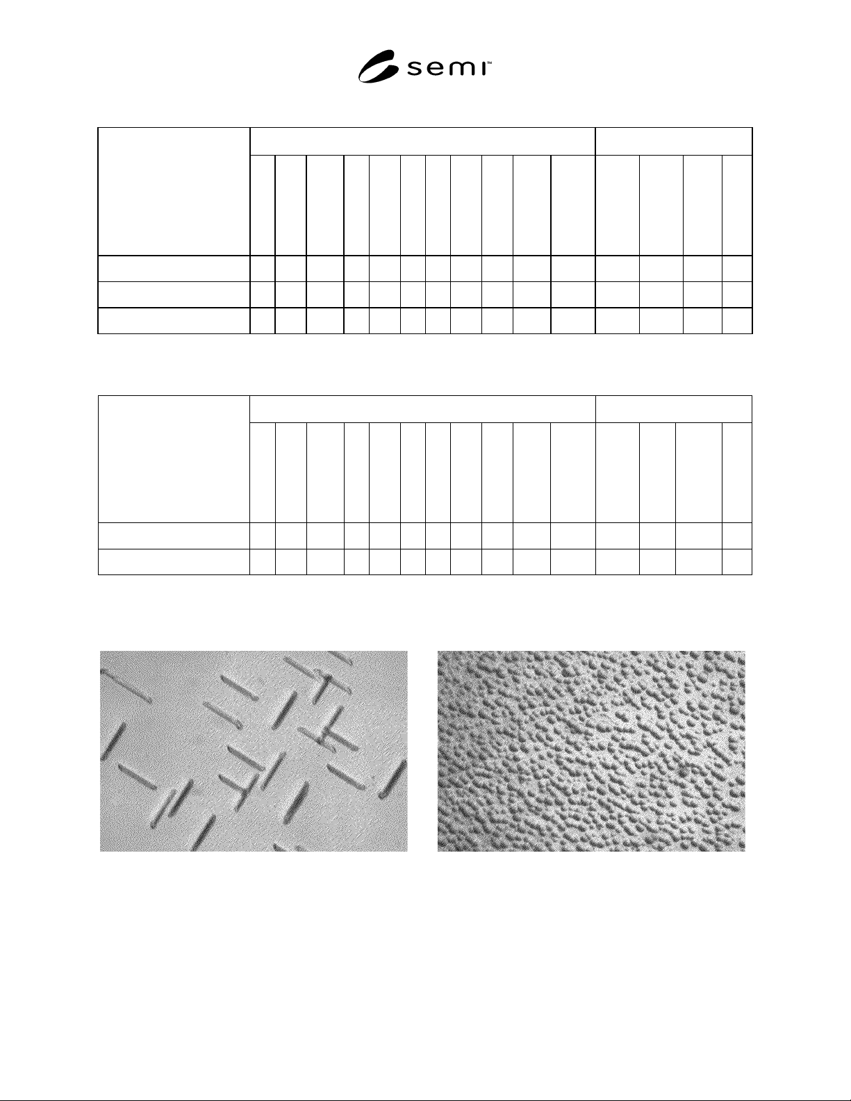
type, 10 Ω·cm, (100) Wafer; 1100° C Steam, 80 minute
Oxidation; Copper-3 Etch with Agitation; 2 µm removal
Figure 1
Oxidation Stacking Fault, 500
×
p type, 10 Ω·cm, (111) Wafer; 1100° C Steam, 80 minute
Oxidation; Copper-3 Etch with Agitation; 2 µm removal
Figure 2
Shallow Pits (Haze), 500
×
SEMI MF1809-0704 © SEMI 2003, 2004 6
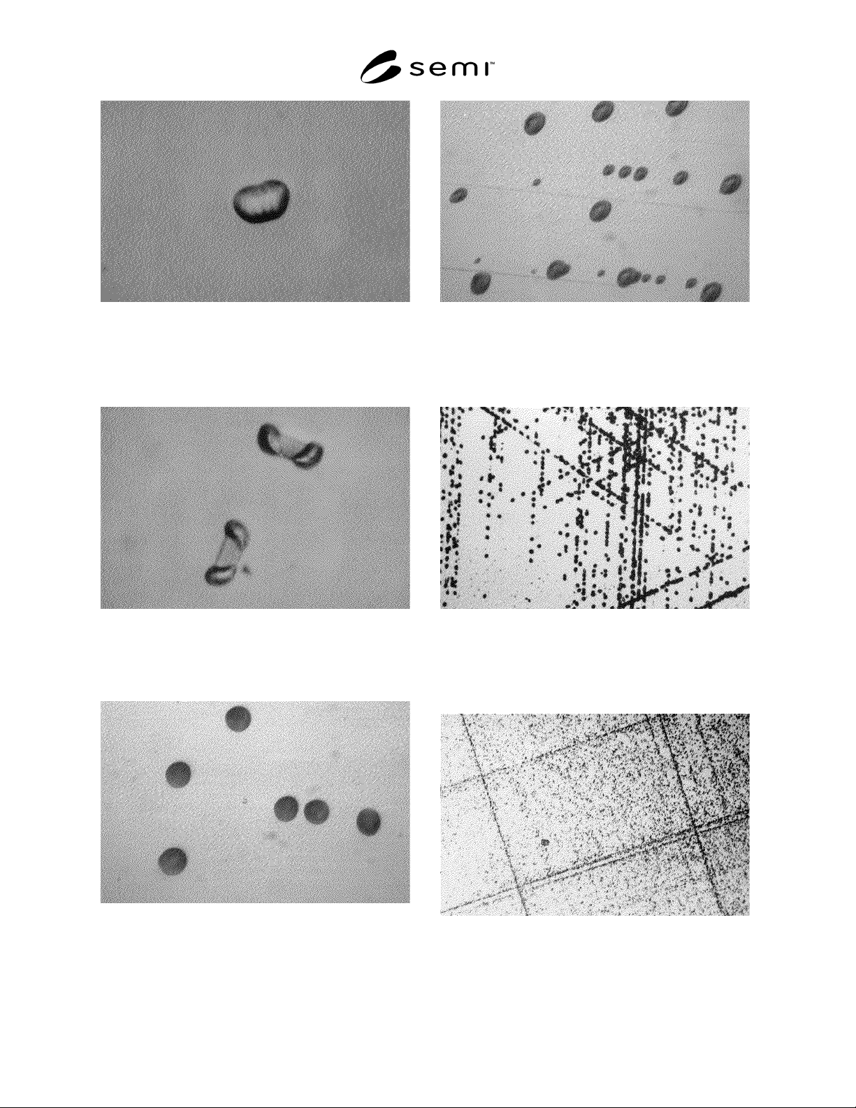
p type, 10 Ω·cm, (100) Wafer; 1100° C Steam, 80 minute
Oxidation; Copper-3 Etch without Agitation; 1 µm removal
Figure 3
Oxidation Stacking Fault, 1000
×
p type, 10 Ω·cm, (100) Wafer; 1100° C Steam, 80 minute
Oxidation; Copper-3 Etch without Agitation; 1 µm removal
Figure 4
Oxidation Stacking Fault, 1000
×
p type, 10 Ω·cm, (111) Wafer; Copper-3 Etch without
Agitation; 10 µm removal
Figure 5
Dislocations, 500
×
p type, 10 Ω·cm, (100) Wafer; Copper-3 Etch without
Agitation; 10 µm removal
Figure 6
Dislocations, 500
×
p type, 10 Ω·cm, (111) Wafer; Copper-3 Etch without
Agitation; 10 µm removal
Figure 7
Slip Dislocations, 500
×
p type, 10 Ω·cm, (100) Wafer; Copper-3 Etch without
Agitation; 10 µm removal
Figure 8
Slip Dislocations, 100
×
SEMI MF1809-0704 © SEMI 2003, 2004 7
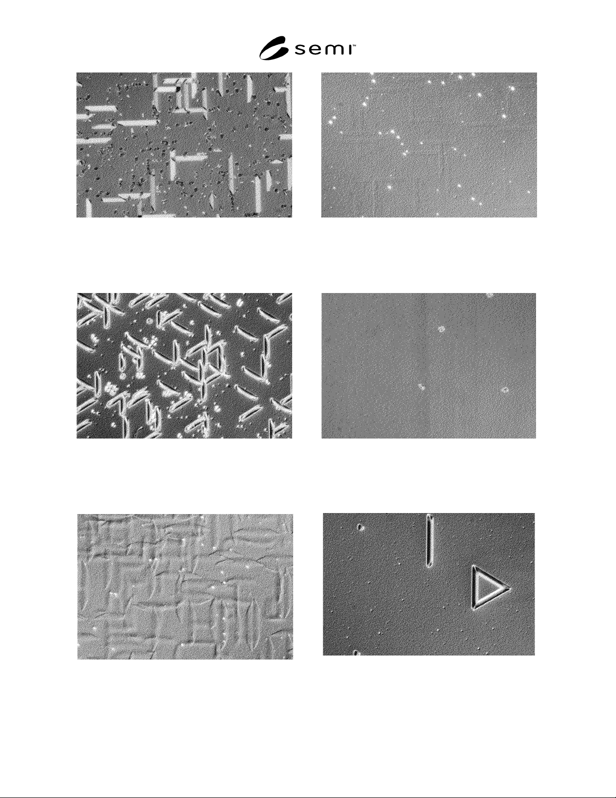
p type, 10 Ω·cm, (100) Wafer; 1100°C, O
2
, 8 hour Oxidation;
Modified Dash Etch; ~ 4 µm removal
Figure 9
Oxidation Induced Stacking Faults, 400
×
n type, 10 Ω·cm, (111) Wafer; 1100°C, O
2
, 8 hour Oxidation;
Modified Dash Etch; ~ 4 µm removal
Figure 10
Oxidation Induced Stacking Faults, 400
×
p type, 0.007 Ω·cm, (100) Wafer; 1100°C, O
2
, 8 hour
Oxidation; Modified Dash Etch; ~ 5 µm removal
Figure 11
Oxidation Induced Stacking Faults, 400
×
p type, <0.02 Ω·cm, (100) Wafer; 1100°C, O
2
, 8 hour
Oxidation; Modified Dash Etch; ~ 5 µm removal
Figure 12
Oxidation Induced Stacking Faults, 400
×
p/p
+
(100) Epitaxial Wafer; Modified Dash Etch; ~ 4 µm
removal
Figure 13
Slip Dislocations, 400
×
n/n
+
(111) Epitaxial Wafer; Modified Dash Etch; ~ 4 µm
removal
Figure 14
Slip Dislocations, Epitaxial Stacking Faults, and
Shallow Pits, 400
×