semi合集-English.pdf - 第5310页
SEMI M49-0704 © SEMI 2001, 2004 9 Item Recommended Specification Comments References 1.3 Wafer Char acteristics – electrical, optical 1.3.1 Electrical Resistivity of Wafers, Conductivity Type 0.5 m Ω cm – intrinsic, p-, …
SEMI M49-0704 © SEMI 2001, 2004 8
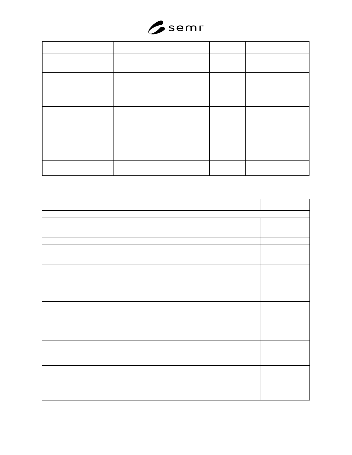
Item Recommended Specification Comment References
5.10 Operating Sequence complete remote control : recipe download,
start, stop, define data evaluation via
SECS/GEM
SEMI E5
5.11 Data Interfaces - SECS/GEM
- optional additionally a mass data standard
transfer protocol (e.g. FTP)
SEMI E5
www.w3.org/Protocols/rfc95
9
5.12 Material Tracking System
Support
required, details user specific
5.13 Output File Format standardized formats:
- ASCII or XML for measurement results
- IEEE for raw data (floating point)
- JPEG (or equivalent) for raw data (image
data)
ISO/IEC 8859, ISO/IEC
10646-1
www.w3.org, ISO 8879
IEEE 754, IEEE 854
ISO/IEC 10918
5.14 Network Communications
Standards Support
Ethernet, Fast Ethernet IEEE 802
5.15 SECS/GEM required SEMI E5
5.16 ARAMS required SEMI E58
NOTE 1: The particulate contamination PWP value given for the backside has not been established in commercial practice and is under further
consideration by the SEMI Silicon Wafer Committee.
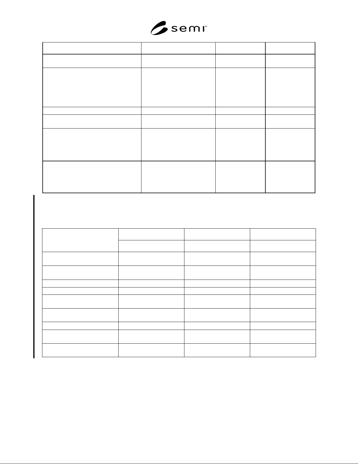
Table 2 Materials to be Measured
Item Recommended Specification Comments References
1 WAFERS
1.1 Kind of Wafers monocrystalline, unpatterned
silicon wafers with layers as
specified in Table 2, Item 1.3.4
SEMI M1
(SEMI M8)
(SEMI M11)
1.2 Wafer Characteristics – dimensional
1.2.1 Wafer Diameter 200 or 300 or 200+300 mm
nominal
SEMI M1
SEMI MF2074
DIN 50441-4
1.2.2 Wafer Thickness 700–850 µm For reclaim wafers
(performance as
outlined in Table 3
might be reduced):
200 mm: 600–850 µ
300 mm: 650–850 µm
SEMI MF1530
DIN 50441-1
1.2.3 Edge Shape rounded SEMI M1
DIN 50441-2
SEMI MF928
1.2.4 Wafer Shape Range 200 mm wfrs: warp <= 100 µm,
300 mm wfrs: warp <= 200 µm
SEMI M1
SEMI MF1390
DIN 50441-5
1.2.5 Fiducial 200 mm wfrs: notch or flat
300 mm wfrs: notch
SEMI M1
SEMI MF671
SEMI MF1152
(DIN 50441-4)
1.2.6 ID Mark(s) 200 mm wfrs: user specific
300 mm wfrs: according to SEMI
standards
content, type location
of ID mark to be
specified
SEMI M1.15
SEMI M12
SEMI M13
SEMI T7
SEMI M49-0704 © SEMI 2001, 2004
9
Item Recommended Specification Comments References
1.3 Wafer Characteristics – electrical,
optical
1.3.1 Electrical Resistivity of Wafers,
Conductivity Type
0.5 mΩcm – intrinsic, p-, n-type Res: SEMI MF673
DIN 50445
SEMI MF84
DIN 50431
Type: SEMI MF42 or
DIN50432
1.3.2 Thermal Donors annealed and not annealed
1.3.3 Wafer Charge no effect with respect to
measurement
1.3.4 Layers (LTO, poly-Si), Epi LTO: thickness: 150 – 900 nm
uniformity: ≤ 10%
poly-Si: thickness: ≤ 2 µm
uniformity: < 20%
Epitaxial layer: customer specific
1.3.5 Wafer Surface Conditions front surface: polished, annealed,
or epitaxial layer
back surface: polished, acid
and/or caustic etched, layers
according to Item 1.3.4
optional conditions of
both surfaces: etched,
lapped, as cut
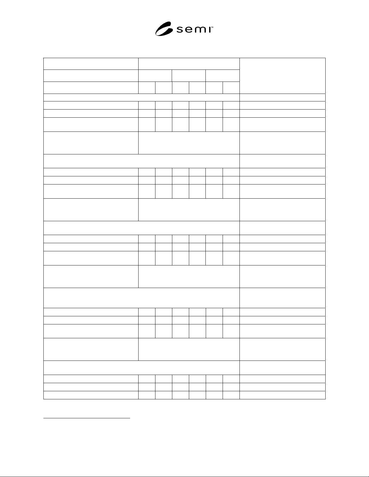
Table 3 Metrology Specific Equipment Characteristics
1. REFERENCE WAFER PROPERTIES (These wafer specifications refer only to wafers to be used for verifying the
performance of the measurement equipment, see Section 6.5.18. They do not refer to product wafers.)
130 nm node 90 nm node 65 nm node
Property
nominal nominal nominal
1.1 Thickness (200 mm wafers),
µm
725 725 725
1.2 Thickness (300 mm wafers),
µm
775 775 775
1.3 GBIR, nm 1000 1000 1000
1.4 Site Size local flatness, mm
2
25*25 26*8 26*8
1.4.1 SBIR, including
partial sites, nm
250 140 125
1.4.2 SFQR, including
partial sites, nm
130 60 45
1.5 Warp, µm
30 30 30
1.6 Nanotopography, 2 mm, P-V,
nm, at 0.05% defective area
20 16 10
1.7 Nanotopography, 10 mm, P-V,
nm, at 0.05% defective area
70 50 35
SEMI M49-0704 © SEMI 2001, 2004 10
2. MEASUREMENT FUNCTIONS
Item Recommended Specification
Technology Generation 130 nm 90 nm
9
65 nm
9
Grade A B A B A B
Comments and References
2.1.1 Thickness (Center Point Thickness) SEMI M1, SEMI MF1530
2.1.1.1 Level 3 Variability σ
3
(µm, 1 σ) ≤ 0.5 ≤ 1 ≤ 0.5 ≤ 1 ≤ 0.5 ≤ 1
2.1.1.2 Matching Tolerance ∆
m
(µm) ≤ 0.75 ≤ 1.5 ≤ 0.75 ≤ 1.5 ≤ 0.75 ≤ 1.5
2.1.1.3 Bias (µm) ≤ 0.75 ≤1.5 ≤ 0.75 ≤ 1.5 ≤ 0.75 ≤ 1.5
target until certified reference
materials are available
2.1.1.4 Spatial Bandwidth
f
min
(mm
–1
)
f
max
(mm
–1
)
0
1
Nominal value ± 5% tolerance
2.1.2 Global Flatness (GBIR) SEMI M1 Appendix 1;
SEMI MF1530; JEIDA 43
2.1.2.1 Level 3 Variability σ
3
(nm, 1 σ) ≤ 30 ≤ 65 ≤ 30 ≤ 65 ≤ 30 ≤ 65
2.1.2.2 Matching Tolerance ∆
m
(nm) ≤ 50 ≤ 100 ≤ 50 ≤ 100 ≤ 50 ≤ 100
2.1.2.3 Bias (nm)
≤ 50 ≤ 100 ≤ 50 ≤ 100 ≤ 50 ≤ 100
target until certified reference
materials are available
2.1.2.4 Spatial Bandwidth
f
min
(mm
–1
)
f
max
(mm
–1
)
0
1
Nominal value ± 5% tolerance
2.1.3 Local Flatness (SBIR) SEMI M1 Appendix 1; SEMI
MF1530; JEIDA 43; DIN 50441-5
2.1.3.1 Level 3 Variability σ
3
(nm, 1 σ) ≤ 8 ≤ 17 ≤ 4.7 ≤ 9.3 ≤ 4.2 ≤ 8.3
2.1.3.2 Matching Tolerance ∆
m
(nm) ≤ 12 ≤ 26 ≤ 7 ≤ 14 ≤ 6.3 ≤ 12.5
2.1.3.3 Bias (nm)
≤ 12 ≤ 26 ≤ 7 ≤ 14 ≤ 6.3 ≤ 12.5
target until certified reference
materials are available
2.1.3.4 Spatial Bandwidth
f
min
(mm
–1
)
f
max
(mm
–1
)
0
1
Nominal value ± 5% tolerance
2.1.4 Local Flatness (SFQR) Specifications apply on a site-by-site
basis; SEMI M1 Appendix 1; SEMI
MF1530; JEIDA 43; DIN 50441-5
2.1.4.1 Level 3 Variability σ
3
(nm, 1 σ) ≤ 4.5 ≤ 9 ≤ 2 ≤ 4 ≤ 1.5 ≤ 3
2.1.4.2 Matching Tolerance ∆
m
(nm) ≤ 7 ≤ 13 ≤ 3 ≤ 6 ≤ 2.3 ≤ 4.5
2.1.4.3 Bias (nm)
≤ 7 ≤ 13 ≤ 3 ≤ 6 ≤ 2.3 ≤ 4.5
target until certified reference
materials are available
2.1.4.4 Spatial Bandwidth
f
min
(mm
–1
)
f
max
(mm
–1
)
0
1
Nominal value ± 5% tolerance
2.1.5 Shape (Warp, GMLYMER) SEMI M1 Appendix 2; SEMI
MF1390; JEIDA 43; DIN 50441-5
2.1.5.1 Level 3 Variability σ
3
(µm, 1 σ) ≤ 1 ≤ 2 ≤ 1 ≤ 2 ≤ 1 ≤ 2
2.1.5.2 Matching Tolerance ∆
m
(µm) ≤ 1.5 ≤ 3 ≤ 1.5 ≤ 3 ≤ 1.5 ≤ 3
2.1.5.3 Bias (µm) ≤ 1.5 ≤ 3 ≤ 1.5 ≤ 3 ≤ 1.5 ≤ 3
9 The values for variability, matching and bias for the 90 and 65 nm technology nodes are rounded to one significant decimal digit for those
parameters which scale with the technology generations. Otherwise the values for the 130 nm genertaion are repeated.