semi合集-English.pdf - 第1057页
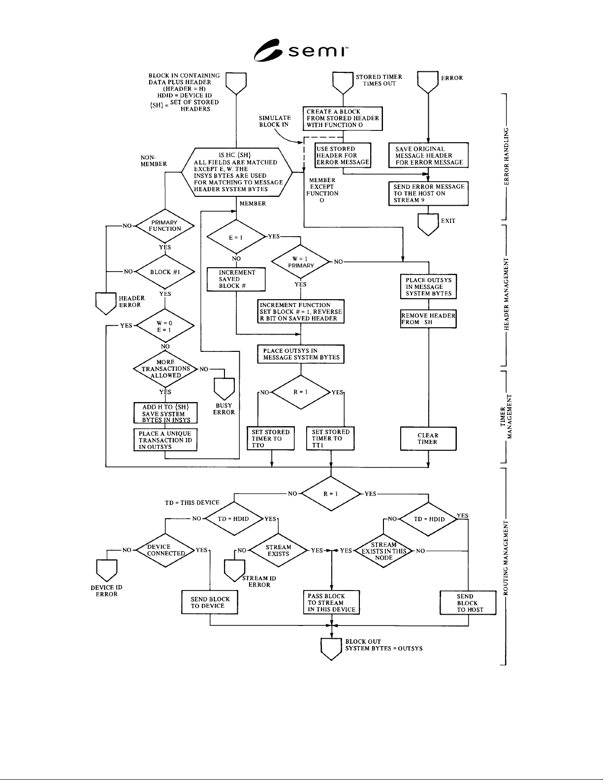
SEMI E4-0699 © SE MI 1980, 1999 19 Figure R1-8 General Node Transa ction Algorith m

SEMI E4-0699 © SEMI 1980, 1999 18
be assumed that an error has occurred and the receiving
machine should release any memory it may be holding
for the transaction. If memory were to remain allocated
to incomplete transactions, conceivably the receiving
machine could run out of available memory and would
be unable to function properly. For this reason, the error
detection of incomplete transactions is an essential part
of the message transaction protocol in SECS-I.
R1-7.2 The message transaction protocol is based on a
system of timers called transaction timers. These timers
are maintained in software and are associated with a
given transaction. Once a transaction is begun, there
will exist a timer on the time interval between all blocks
of the transaction independent of the direction of the
message. The machine that expects to receive a block
has the burden of timing and error detection. Timers are
required in any machine that (1) makes a request and
expects to receive data back; (2) must receive multiple
block requests; or (3) sends data and expects an
acknowledgement. A machine may require several
transaction timers if it can conduct multiple transactions
at one time on one port or has multiple ports. A
message timer will exist for each link involved in the
transaction. This allows the error detection to identify
the particular link which has failed.
R1-7.3 A general algorithm can be constructed to
handle an arbitrary number of SECS ports. Such an
algorithm is presented in the form of a flow chart in
Figure R1-8. There is one such algorithm for each
device ID. The algorithm handles all SECS data blocks
that enter, leave or pass the device ID. A new block
causes the procedure to be executed starting from the
point marked "block in" and continues until the point
marked "block out." The block of data will then be
directed to the proper destination.
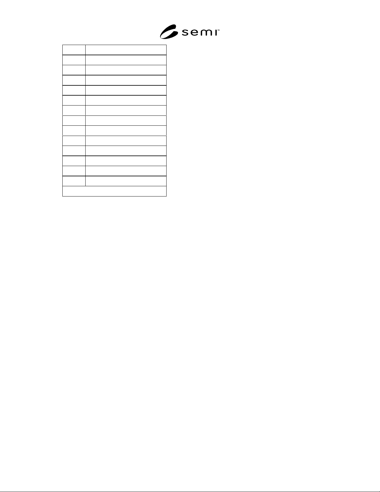
R1-7.4 This algorithm makes use of a stored version of
the message header for each transaction being handled.
The stored header may be visualized as shown in Figure
R1-9. The stored header has two system areas and an
associated transaction timer. The two system areas are
required to keep the incoming and the outgoing system
areas independent in coding, yet related in meaning.
The two system areas are referred to by the state of the
R-bit in the message block header. One area is related
to R = 0 and the other R = l. When a prime message is
received that requires a reply, the system bytes from the
block are stored in the system area corresponding to the
opposite state of the R bit on the message. When the
reply is sent, the system bytes are used from the store
system bytes corresponding to the same R-bit as the
reply. The system area corresponding to the same R-bit
as the message is called OUTSYS while the system
area corresponding to the opposite R-bit is called
INSYS.
R1-7.5 When a block is presented to this algorithm, the
first task is to determine if the block is part of an
ongoing transaction, the first block of a new
transaction, or some other unknown block. This test is
accomplished by comparing the header of the block
with the stored headers. If a match is not found, then a
check is made to see if the block is the first of a primary
message. If this is true, then a new header is added to
the stored header list. If the primary message is only
one block long and requires no reply, then no stored
header is created. When a match is found, the algorithm
modifies the stored header so that it will look like the
next block of the transaction to be expected. On all
blocks requiring a stored header, except the last, a
transaction timer is set to a timeout value prior to
sending the block to its destination. The last part of the
algorithm directs the block to its destination or detects
an error in the destination.
R1-7.6 Error recovery is an important part of the
algorithm to ensure that the system will remain
operational in spite of bad data blocks. For any block
that does not pass the tests described in the algorithm,
the header of the message is saved and sent in the host
direction on a Stream 9 error message. This information
can be useful in tracking down the source of the error.
Another type of error occurs when one of the
transaction timers times out. Such an error message
means that the transaction has been interrupted. An
error message is formed which sends the stored header
in the host direction on Stream 9. The stored header and
the timer are then released. This procedure aids in
keeping software cleared and ready in case of
difficulties in the network.
SEMI E4-0699 © SEMI 1980, 199919
Figure R1-8
General Node Transaction Algorithm
SEMI E4-0699 © SEMI 1980, 1999 20
R Device ID
Device ID
W STREAM
FUNCTION
EBlock No.
Block No.
S1(R=0)
S2(R=0)
S3(R=0)
S4(R=0)
S1(R=1)
S2(R=1)
S3(R=1)
S4(R=1)
Transaction Timer
Figure R1-9
Stored Header Model
NOTICE: These standards do not purport to address
safety issues, if any, associated with their use. It is the
responsibility of the user of these standards to establish
appropriate safety and health practices and determine
the applicability of regulatory limitations prior to use.
SEMI makes no warranties or representations as to the
suitability of the standards set forth herein for any
particular application. The determination of the
suitability of the standard is solely the responsibility of
the user. Users are cautioned to refer to manufacturer’s
instructions, product labels, product data sheets, and
other relevant literature respecting any materials
mentioned herein. These standards are subject to
change without notice.
The user’s attention is called to the possibility that
compliance with this standard may require use of
copyrighted material or of an invention covered by
patent rights. By publication of this standard, SEMI
takes no position respecting the validity of any patent
rights or copyrights asserted in connection with any
item mentioned in this standard. Users of this standard
are expressly advised that determination of any such
patent rights or copyrights, and the risk of infringement
of such rights, are entirely their own responsibility.
Copyright by SEMI® (Semiconductor Equipment and Materials
International), 3081 Zanker Road, San Jose, CA 95134. Reproduction o
f
the contents in whole or in part is forbidden without express written
consent of SEMI.