semi合集-English.pdf - 第5768页
SEMI P21-92 © SEMI 1992, 2003 3 Figure 1

SEMI P21-92 © SEMI 1992, 2003 2
3.4 Pattern Stitching Accuracy
3.4.1 Definition
• Position errors at the stitching boundary of writing
fields, stripes, and shots.
3.4.2 Expression
• |average value| 1 + 3 σµm (X and Y direction
separately) measured area and number of sampling
points should be clearly described.
3.4.3 Measurement
• Optical coordinates measurement
• Electron beam coordinate measurement
• Coordinates measurement done by self-diagnostic
feature of writing equipment.
• Vernier measurement
• Boundary measurement by SEM image
3.4.4 Requirement
• The pattern should be cross or L marks in both
sides adjacent to the stitching boundary for
coordinate measurement.
• When the optical microscope is used for
measurement, the vernier pattern should be used.
4 Notice
4.1 The following subjects should be agreed upon
beforehand between users and makers in order to
evaluate the above-mentioned writing precision and
accuracy item.
4.1.1 Process Requirements
• Resist Materials
• Coating Condition
• Development Condition
• Process Sequence
• Mask Substrate and Chrome Thin Film Materials
4.1.2 Test Pattern
4.1.3 Measurement Procedure
5 Others
5.1 The following items are not specified in these
guidelines, still it is preferable that these items are
agreed upon beforehand between user and supplier.
5.1.1 Pattern coordinates
5.1.2 Pattern position accuracy
5.1.3 Long-term stability of accuracy
5.1.4 Particles
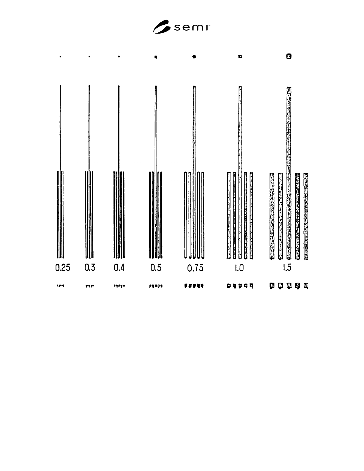
SEMI P21-92 © SEMI 1992, 2003 3
Figure 1
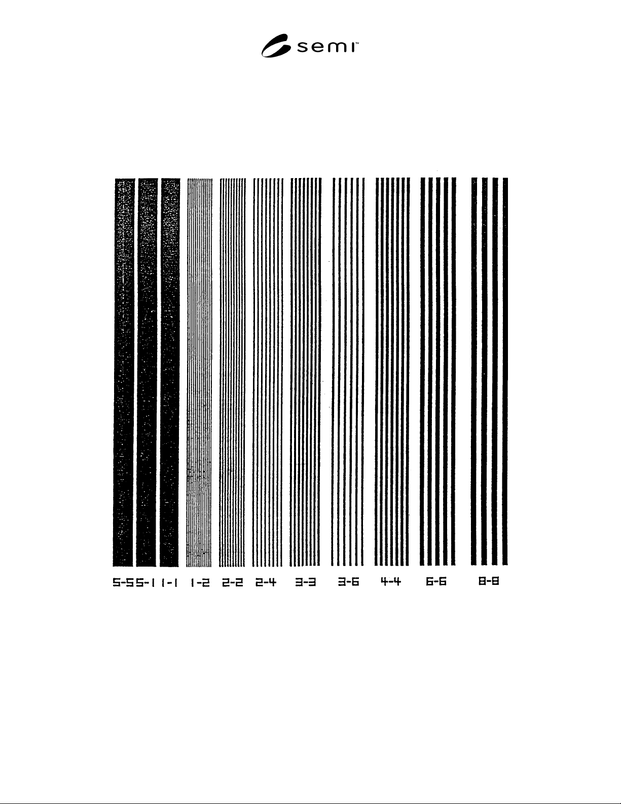
SEMI P21-92 © SEMI 1992, 2003 4
Figure 2