semi合集-English.pdf - 第4957页
SEMI M11-0704 © SEMI 1988, 2004 14 4.4 Othe r terms are de fined as follows: 4.4.1 autod oping, of an epit axial layer — incorporatio n of dopant origi n ating from the substrate into the epitaxial layer. Also called sel…
SEMI M11-0704 © SEMI 1988, 2004 13
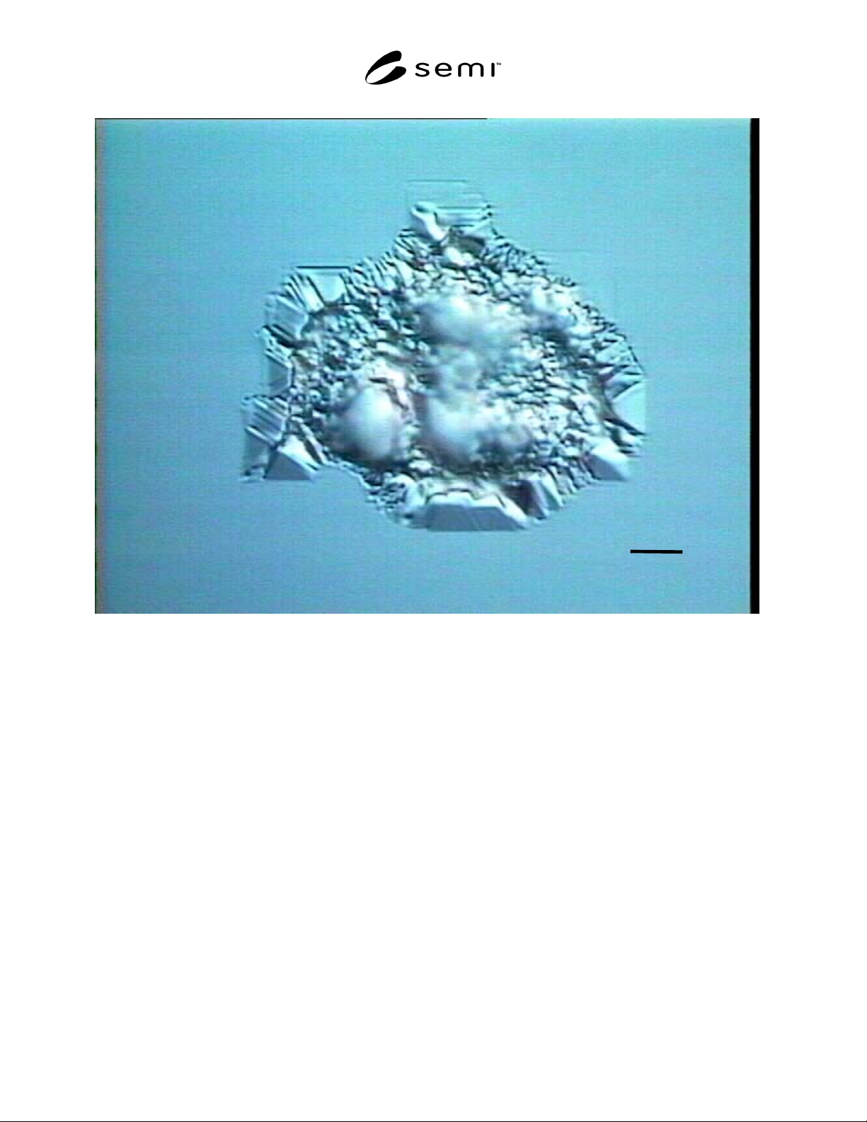
Figure 11
A Polysilicon Epitaxial Stacking Fault is a defect that covers a large area and is covered or surrounded by
ESFs. This classification is used when the surface appears to be poly-crystalline rather than single crystal. It
is almost always a Large Area Defect and is caused by a large particle that may still be visible (see Buried
Particle). Magnification 1500 times using Nomarski Interference Microscopy. Approximate SSIS event size,
440 µm
5
µ
m

SEMI M11-0704 © SEMI 1988, 2004 14
4.4 Other terms are defined as follows:
4.4.1 autodoping, of an epitaxial layer —
incorporation of dopant originating from the substrate
into the epitaxial layer. Also called self-doping.
NOTE 3: Sources of autodoping can be the back and front
surfaces and edges of the substrate, other substrates in the
reactor, the susceptor, or other parts of the deposition
assembly.
4.4.2 chemical vapor deposition, in semiconductor
technology — a process in which a controlled chemical
reaction produces a thin surface film.
NOTE 4: Epitaxial growth is an example of a special case of
chemical vapor deposition (CVD).
4.4.3 edge crown — the difference between the surface
elevation 1/8 inch (3.2 mm) from the edge of the wafer
and the elevation at the wafer edge.
4.4.4 effective layer thickness, of an epitaxial layer —
the depth from the front surface in which the net carrier
density is within the specified limits.
4.4.5 epi profile slope, of an epitaxial layer — the
difference between the net carrier density at 0.75 of the
layer thickness and the net carrier density at 0.25 of the
layer thickness divided by one-half the layer thickness:
t
NN
tt
5.0
25.075.0
slopeprofileepi
−
=
m. kness,layer thic
and,
3-
cmdensity,carriernet
:where
µ
=
=
t
N
4.4.6 epitaxial layer — a layer of single crystal
semiconductor material grown on a host substrate
which determines its orientation.
4.4.7 epitaxy — the growth of a single crystal layer on
a substrate of the same material, homoepitaxy; or on a
substrate of different material with a compatible crystal
structure, heteroepitaxy.
4.4.8 flat zone, of an epitaxial layer — the depth from
the front surface to the point where the net carrier
density is 20% greater than or less than the average net
carrier density (see Section 7.3.2) of the region between
0.25 and 0.75 of the layer thickness.
4.4.9 laser light scattering event — a signal pulse that
exceeds a preset threshold, generated by the interaction
of a laser beam with a discrete scatterer at a wafer
surface as sensed by a detector.
4.4.10 thickness, of an epitaxial layer — the distance
from the surface of the wafer to the layer-substrate
interface.
4.4.11 transition width, of an epitaxial layer deposited
on a more heavily doped substrate of the same
conductivity type — the difference between the layer
thickness as determined by infrared reflectance (see
Section 7.3.1) and the flat zone based on the same
thickness measurement.
5 Ordering Information
5.1 Purchase orders for the epitaxial layer on substrates
furnished to this specification shall include the
following items:
5.1.1 Substrate Characteristics
5.1.2 Epitaxial Layer Characteristics
5.1.2.1 Silicon Source for Epitaxial Growth (if
required) (see Note 3.)
5.1.2.2 Epitaxial Layer Conductivity Type and Doping
Source (see Note 3.)
5.1.2.3 Etch Removal (if required)
5.1.2.4 Epitaxial Layer Center Point Thickness and
Thickness Tolerances
5.1.2.5 Epitaxial Layer Thickness Variation Range
5.1.2.6 Epitaxial Layer Centerpoint Net Carrier
Density and Net Carrier Density Tolerances (see Note
4.)
5.1.2.7 Epitaxial Layer Net Carrier Density Variation
Range
5.1.2.8 Epitaxial Layer Defect Limits
5.1.3 Methods of Test and Measurements (see Section
7.)
5.1.4 Lot Acceptance Procedures (see Section 8.)
5.1.5 Certification (if required) (see Section 9.)
5.1.6 Packing and Marking (see Section 10.)
NOTE 5: The dopant, doping method, and growth method are
difficult to ascertain in the finished wafers. Verification test
procedures or certification of these characteristics shall be
agreed upon between the supplier and the purchaser. (See
Section 9.)
NOTE 6: Care should be taken in converting between carrier
density and resistivity using SEMI MF723. Multiple
conversions may introduce differences in values. For
example, converting from carrier density (C
i
) to resistivity
and back to carrier density (C
f
), may result in C
i
not equaling
C
f
.

SEMI M11-0704 © SEMI 1988, 2004 15
6 Requirements
6.1 As a minimum, the substrate shall conform to
SEMI M1 and the appropriate individual polished
monocrystalline silicon wafer standard.
6.2 Epitaxial wafer defects shall not exceed the limit as
given in Table 1.
6.2.1 Limits for slip, which may require destructive
testing, shall be specified in a purchase order together
with an appropriate test method. In the absence of
another specification, the wafer will contain no slip
lines within the quality area. (See Table 1, Note 1.)
NOTE 7: When an unetched wafer is observed for slip it is
impossible to differentiate between slip and linear misfit lines.
6.3 Layer Thickness Variation — Unless otherwise
specified, the thickness variation shall be determined
from value measured at the center and locations
centered 12 mm ± 1 mm from the periphery, on
diameters both parallel and perpendicular to the
primary flat,
100
tt
tt
(%)Variation
minmax
minmax
×
+
−
=
where t
max
and t
min
denote the maximum and minimum
thickness values measured. The 12 mm locations have
been defined based on instrument processing and
fixturing considerations.
6.4 Layer Net Carrier Density Variation — The net
carrier density variation shall be determined from
values measured at the center and locations with center
of the probe at 12 mm ± 1 mm from the periphery, on
diameters both parallel and perpendicular to the
primary flat,
100
NN
NN
(%)Variation
minmax
minmax
×
+
−
=
where N
max
and N
min
denote the maximum and
minimum values measured. The 12 mm locations have
been defined based on instrument processing and
fixturing considerations.
7 Test Methods and Measurements
7.1 Measurements shall be carried out in conformance
with the specified SEMI Test Methods. Where no
methods are specified or where choices are given, the
supplier and purchaser shall agree in advance on the
means for making the measurement.
7.2 Substrates — Determine in accordance with
methods specified in SEMI M1.
7.3 Epitaxial Layer
7.3.1 Thickness — Determine in accordance with
SEMI MF95 or SEMI MF110.
NOTE 8: In the case of thin layers and graded doping
transitions, SEMI MF95 and SEMI MF110 may not be
suitable. See the scopes of these test methods to determine
their limitations. In all cases, there is a possibility that various
types of infrared reflectance instrumentation may result in
different values of epitaxial layer thickness. Therefore, the
instrumentation used shall be agreed upon between supplier
and purchaser.
7.3.2 Net Carrier Density — Determine by method(s)
agreed upon between supplier and purchaser.
NOTE 9: SEMI MF1392 and SEMI MF1393 are methods for
measuring net carrier density using a mercury probe contact.
If resistivity is measured, as by SEMI MF374 or SEMI
MF525, conversion to dopant density shall be made using
SEMI MF723. Net carrier density of very heavily doped
layers (or substrates) may be found using SEMI MF398. Net
carrier density profiles may be determined directly in
accordance with SEMI MF1392 or SEMI MF1393 or
indirectly in accordance with SEMI MF672, with conversion
from resistivity to net carrier density in accordance with
SEMI MF723. If the method used for determining the net
carrier density profile is not the same as that used to
determine the center-point net carrier density, correlation
between the two methods used shall be established.
7.3.3 Epitaxial Wafer Defects — Determine in
accordance with the methods given in Table 1.
7.3.3.1 Surface inspection shall be performed before
any other testing. Wafers may be cleaned prior to
inspection to minimize difficulty in the visual
inspection of defects other than foreign matter.
7.3.3.2 Slip — Determine by methods agreed upon
between supplier and purchaser.
7.3.3.3 Automatic surface inspection technology is
being developed to detect and discriminate surface
defects. The extended definitions in Section 4.3 are
intended to facilitate this development.
NOTE 10: For observation of gross slip, examination of the
epitaxial layer under the illumination conditions specified in
Section 12.2 of SEMI MF523 may suffice. For more
demanding applications, it may be desirable to etch the
surface in accordance with SEMI MF1726 prior to the visual
inspection.
7.4 If substrates of different type and net carrier
density than the product substrates are to be used for
deposition control, their type, resistivity, and quantity
per run or lot shall be agreed upon between supplier and
purchaser.