semi合集-English.pdf - 第5453页
SEMI M61-0705 © SEMI 2005 2 4.2.2 buried layer — a diffused region in a substrate that is, or is intended to be, covered with an epitaxial layer. 4.2.3 pattern distortio n ratio — absolute m agnitude of the quotient o f …

SEMI M61-0705 © SEMI 2005 1
SEMI M61-0705
SPECIFICATION FOR SILICON EPITAXIAL WAFERS WITH BURIED
LAYERS
This standard was technically approved by the global Silicon Wafer Committee. This edition was approved
for publication by the global Audits and Reviews Subcommittee on May 20, 2005. It was available at
www.semi.org in June 2005 and on CD-ROM in July 2005.
1 Purpose
1.1 Some silicon epitaxial wafers are supplied with buried layers under the epitaxial film. This specification covers
the properties of such epitaxial wafers that pertain to the buried layer.
2 Scope
2.1 This specification defines the properties of silicon epitaxial wafers with buried layers that relate to the
characteristics of photolithography, buried layer, and buried layer pattern after the deposition of the epitaxial layer.
2.2 This specification is intended to be used with the polished wafer specification (SEMI M1) and the epitaxial
wafer specification (SEMI M2), which define the properties of the substrate and the epitaxial layer, respectively.
2.3 The EDI Code List for items appropriate to epitaxial wafers with buried layers is given in SEMI M18.
NOTICE: This standard does not purport to address safety issues, if any, associated with its use. It is the
responsibility of the user of this standard to establish appropriate safety and health practices and determine the
applicability of regulatory or other limitations prior to use.
3 Referenced Standards and Documents
3.1 SEMI Standards
SEMI M1 — Specifications for Polished Monocrystalline Silicon Wafers
SEMI M2 — Specifications for Silicon Epitaxial Wafers for Discrete Device Applications
SEMI M18 —Format for Silicon Wafer Specification Form for Order Entry
SEMI M20 — Practice for Establishing a Wafer Coordinate System
SEMI M59 — Terminology for Silicon Technology
SEMI MF26 — Test Methods for Determining the Orientation of a Semiconductive Single Crystal
3.2 ANSI Standard
1
ANSI/ASQC Z1.4 — Sampling Procedures and Tables for Inspection by Attributes
3.3 JEITA Standard
2
EM-3501 — Standard methods for determining the orientation of a semiconductor silicon single crystal
NOTICE: As listed or revised, all documents cited shall be the latest publications of adopted standards.
4 Terminology
4.1 General terminology for silicon wafers and silicon technology is covered in SEMI M59 to be published in
March).
4.2 Terms related to epitaxial wafers with buried layers are as follows:
4.2.1 alignment precision — pattern displacement in first mask photolithography process.
1 American National Standards Institute, New York Office: 11 West 42nd Street, New York, NY 10036, USA. Telephone: 212.642.4900; Fax:
212.398.0023 Website:
www.ansi.org
.
2 Japan Electronics and Information Technology Industries Association, 3rd floor, Mitsui Sumitomo Kaijo Bldg. Annex, 11, Kanda-Surugadai 3-
chome, Chiyoda-ku, Tokyo 101-0062, Japan. Tel:81.3.3518.6434; Fax:81.3.3295.8727
Website:www.jeita.or.jp
SEMI M61-0705 © SEMI 2005 2
4.2.2 buried layer — a diffused region in a substrate that is, or is intended to be, covered with an epitaxial layer.
4.2.3 pattern distortion ratio — absolute magnitude of the quotient of (1) the difference between the width of the
pattern on the substrate and the width of the pattern on the top surface of the epitaxial layer and (2) the thickness of
the epitaxial layer.
4.2.4 pattern shift ratio — lateral distance between the center point of the pattern on the surface of the substrate and
the center point of the pattern on the surface of the epitaxial layer divided by the epitaxial layer thickness.
4.2.5 pattern step height — difference in vertical position of the diffused (buried layer) surface and the original
substrate surface, after removal of oxide.
5 Ordering Information
5.1 Purchase orders for silicon epitaxial wafers furnished to this specification shall include the items indicated in
sections 4-1 through 4-3 of Part 4 of the Specification Format for Order Entry (for Epitaxial Wafer with Buried
Layer) shown in Table 1. Other specified characteristics, as required, may be added in section 4-4 of the format.
5.2 In addition, the purchase order shall include
the material in Part 1 (General Information) of the Specification Format for Order Entry, in SEMI M1,
specifications for the substrate wafer of the appropriate characteristics as defined in Part 2 (Polished Wafer or
Substrate) also in SEMI M1, and
specifications for the epitaxial layer as defined in SEMI M2.
NOTE 1: Note that the orientation of single crystal is differently specified in SEMI MF26 and JEITA EM-3501.
5.3 The following items must also be included in the purchase order:
5.3.1 Lot acceptance procedures.
5.3.2 Certification (if required).
5.3.3 Packing and marking requirements.
Table 1 Specification Format for Order Entry
Part 4 Epitaxial Wafer with Buried Layer
ITEM SPECIFICATION
1. PHOTOLITHOGRAPHY CHARACTERISTICS
4-1.1 Mask ID [ ] Number: [ ]; [ ]None
4-1.2 Alignment Precision X max [ ] µm, Y max [ ] µm;
Reference Point (Wafer Coordinate System): x [ ] mm, y [ ] mm;
max [ ]
4-1.3 Pattern Line Width Tolerance Tolerance ± [ ] µm
2. BURIED LAYER CHARACTERISTICS
4-2.1 Dopant [ ]B; [ ]P; [ ]Sb; [ ]As
4-2.2 Diffusion Depth (x
j
) Nominal [ ] ± Tolerance [ ] µm
4-2.3 Sheet Resistance Nominal [ ] ± Tolerance [ ] /sq
4-2.4 Pattern Step Height Nominal [ ] ± Tolerance [ ] nm
4-2.5 Defect Density (Before Epi) Not greater than [ ]/cm
2
3. BURIED LAYER PATTERN CHARACTERISTICS AFTER EPI
4-3.1 Pattern Shift Ratio Nominal [ ] ± Tolerance [ ]
4-3.2 Pattern Distortion Ratio Max. [ ]
4. OTHER CHARACTERISTICS
SEMI M61-0705 © SEMI 2005 3
ITEM SPECIFICATION
6 Requirements
6.1 General Characteristics
6.1.1 The epitaxial wafers with buried layers shall meet all requirements specified in the purchase order including
those requirements related to both the substrate wafer and epitaxial layer properties.
6.2 Photolithography Characteristics
6.2.1 The identified mask shall be used in making the pattern for the diffused layers.
6.2.2 The alignment precision shall meet the specified requirements as follows:
6.2.2.1 The values of X and Y, the displacement of the center of the pattern from a reference position defined in the
wafer specification in terms of the wafer coordinate system defined in SEMI M20, shall not exceed the maximum
values specified.
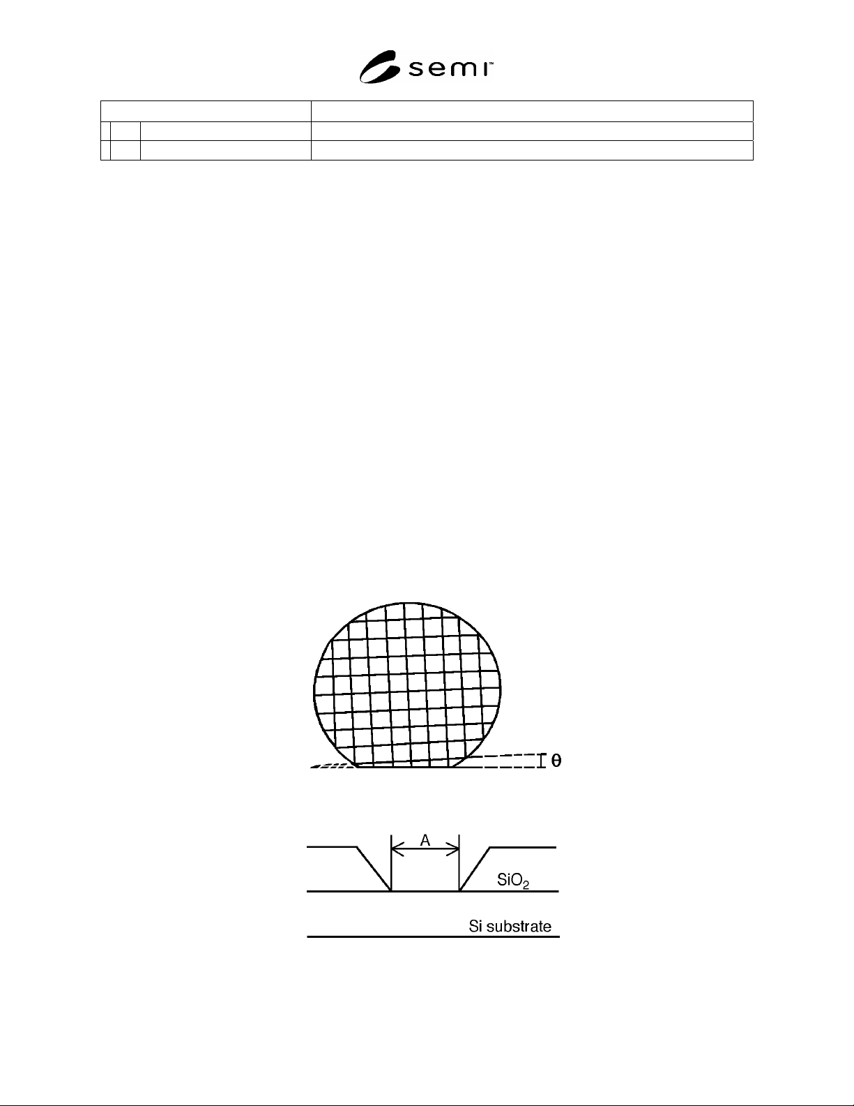
6.2.2.2 The value of θ, the angle between the x-axis of the pattern and the primary orientation flat (see Figure 1)
shall not exceed the maximum value specified.
6.2.3 The pattern line widths (see Figure 2) shall be within the specified tolerance of the desired values.
6.3 Buried Layer Characteristics
6.3.1 The dopant shall be the element specified: boron (B), phosphorus (P), antimony (Sb) or arsenic (As).
6.3.2 The diffusion depth shall fall within the tolerance of the nominal value specified in micrometers (m).
6.3.3 The sheet resistance of the diffused layer shall fall within the tolerance of the value specified in ohms per
square (/sq).
Figure 1
First Mask Showing Angular Displacement
Figure 2
Schematic Diagram Showing Line Width, A, of Pattern on Substrate Wafer