semi合集-English.pdf - 第5956页
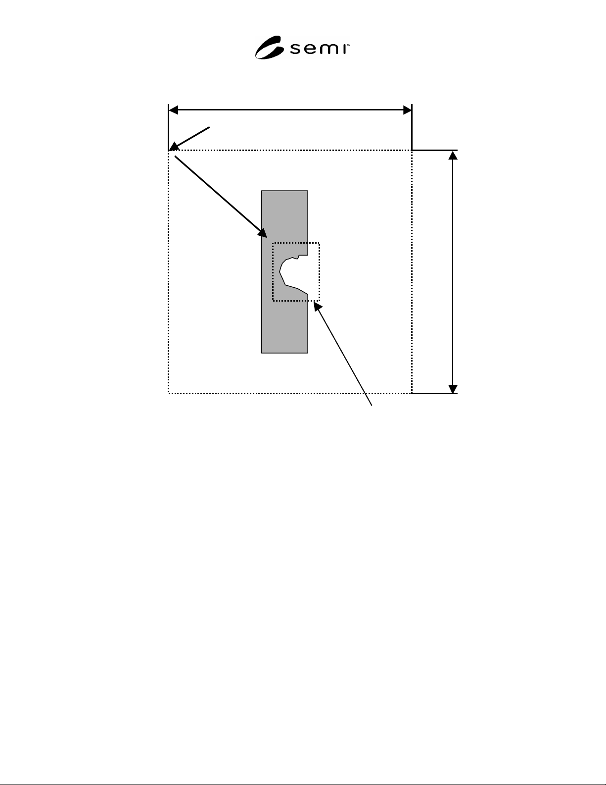
SEMI P41-0304 E © SEMI 2004 16 I ma g e R ef er en c e P o int I mage S iz e X E x p r essi o n M ar k I mage Targe t Pos i ti o n X an d Y Im a g e S iz e Y Figure 12 Image Target NOTICE: SEMI makes no warranties or rep…
SEMI P41-0304
E
© SEMI 2004 15
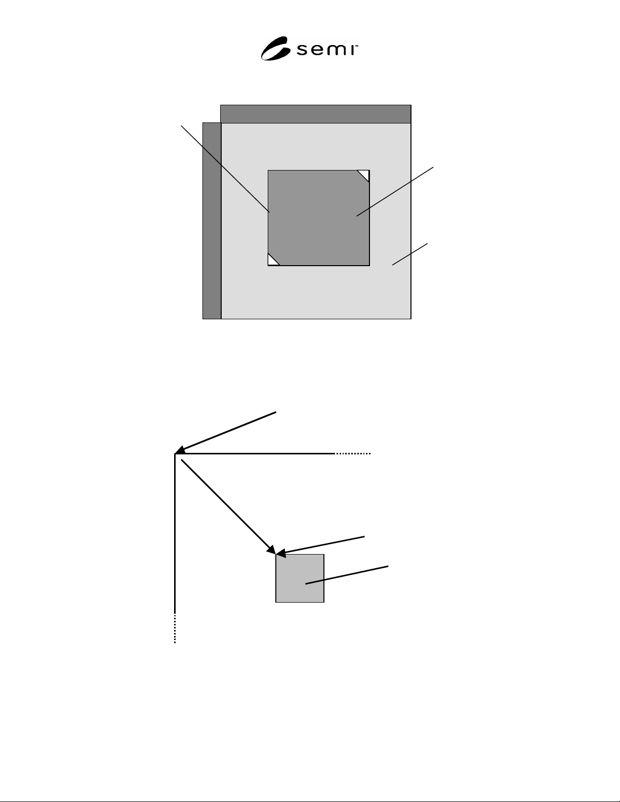
Reference mark
Mask
Stage or Holder
I D
Figure 10
Direction
Image Reference
Image Data
Image Referenc Point
Position Information X and Y
Figure 11
Image Reference
SEMI P41-0304
E
© SEMI 2004 16
Image Reference Point
Image Size X
Expression Mark
Image Target Position X and Y
Image S ize Y
Figure 12
Image Target
NOTICE: SEMI makes no warranties or representations as to the suitability of the standards set forth herein for any
particular application. The determination of the suitability of the standard is solely the responsibility of the user.
Users are cautioned to refer to manufacturer's instructions, product labels, product data sheets, and other relevant
literature, respecting any materials or equipment mentioned herein. These standards are subject to change without
notice.
By publication of this standard, Semiconductor Equipment and Materials International (SEMI) takes no position
respecting the validity of any patent rights or copyrights asserted in connection with any items mentioned in this
standard. Users of this standard are expressly advised that determination of any such patent rights or copyrights, and
the risk of infringement of such rights are entirely their own responsibility.

SEMI P41-0304
E
© SEMI 2004 17
RELATED INFORMATION 1
APPLICATION NOTES
NOTICE: This related information is not an official part of SEMI P41 and was derived from the work of the
originating task force. This related information was approved for publication by full letter ballot procedures on
January 9, 2004.
R1-1 EXAMPLE OF AN XML FILE
<?xml version ="1.0"?>
<MDML data_no = "00001" date_stamp = "03-sep-2003">
<BasicInformation>
<MaskMaterialInformation>
<MaskSize unit = "inch" shape = "Square">
<MaskSize_X>6</MaskSize_X>
<MaskSize_Y>6</MaskSize_Y>
<MaskThickness>0.25</MaskThickness>
</MaskSize>
<MaskAbsorber>AR</MaskAbsorber>
</MaskMaterialInformation>
<DefectInspection preparation_date = "03-sep-2003">
<InspectionTool tool_name = "SEMI-J" tool_no = "001">
<ToolCoordinateInformation>
<CoordinateSystem>TopLeft_0</CoordinateSystem>
<ToolOriginPointInformation>
<ToolOriginPoint>stage top left corner</ToolOriginPoint>
<ToolOriginPosition unit = "micron">
<ToolOriginPosition_X>0</ToolOriginPosition_X>
<ToolOriginPosition_Y>0</ToolOriginPosition_Y>
</ToolOriginPosition>
</ToolOriginPointInformation>
<ToolStageCorrectionInformation>
<ToolStageCorrection unit = "ppm">
<ToolStageCorrection_X>-5</ToolStageCorrection_X>
<ToolStageCorrection_Y>10</ToolStageCorrection_Y>
</ToolStageCorrection>
<ToolStageSkew unit = "microm">
<ToolStageSkewCorrection>2</ToolStageSkewCorrection>
</ToolStageSkew>
</ToolStageCorrectionInformation>
<MaskOriginPointInformation>
<MaskOriginPoint>TopLeft</MaskOriginPoint>
<MaskOriginPosition unit = "micron">
<MaskOriginPosition_X>0</MaskOriginPosition_X>
<MaskOriginPosition_Y>0</MaskOriginPosition_Y>
</MaskOriginPosition>
<ToolOffset unit = "micron">
<ToolOffset_X>30000</ToolOffset_X>
<ToolOffset_Y>30000</ToolOffset_Y>
</ToolOffset>
</MaskOriginPointInformation>
<ToolStageAccuracy unit = "micron">1</ToolStageAccuracy>