semi合集-English.pdf - 第4500页
SEMI D21-1000 © SEMI 1992, 2000 1 SEMI D21-1000 TERMINOLOGY FOR FL A T P ANEL DISPLAY MASKS This term inology was te chnically approv ed by the Gl obal Flat Panel Display Committee a nd is the direct responsi bility of t…
SEMI D20-1000 © SEMI 1993, 2000 2
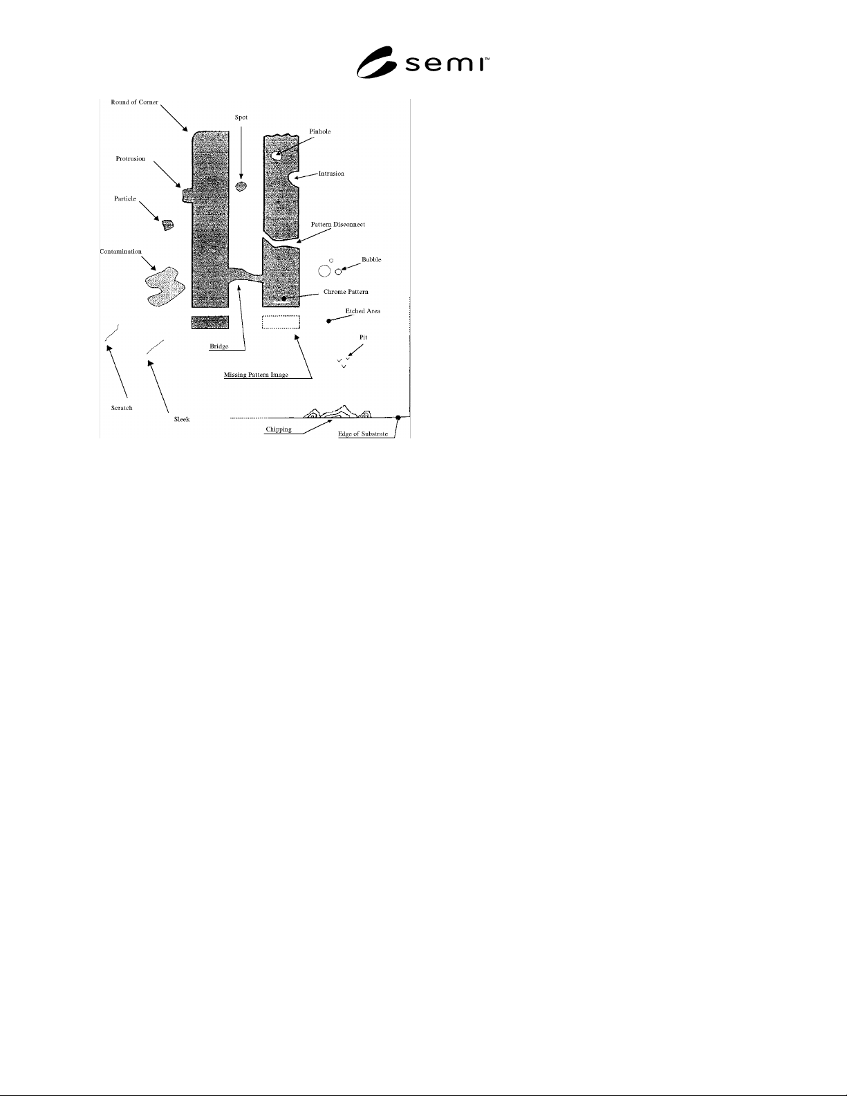
Figure 1
Image of Defects for FPD Mask
NOTICE: The user’s attention is called to the
possibility that compliance with this standard may
require use of copyrighted material or of an invention
covered by patent rights. By publication of this
standard, SEMI takes no position respecting the validity
of any patent rights or copyrights asserted in connection
with any item mentioned in this standard. Users of this
standard are expressly advised that determination of
any such patent rights or copyrights, and the risk of
infringement of such rights, are entirely their own
responsibility.
Copyright by SEMI® (Semiconductor Equipment and Materials
International), 3081 Zanker Road, San Jose, CA 95134. Reproduction o
f
the contents in whole or in part is forbidden without express written
consent of SEMI.
SEMI D21-1000 © SEMI 1992, 20001
SEMI D21-1000
TERMINOLOGY FOR FLAT PANEL DISPLAY MASKS
This terminology was technically approved by the Global Flat Panel Display Committee and is the direct
responsibility of the Japanese Flat Panel Display Materials and Components Committee. Current edition
approved by the Japanese Regional Standards Committee on July 28, 2000. Initially available on SEMI
OnLine September 2000; to be published October 2000. Originally published in 1992.
1 Purpose
1.1 This document defines termino logy for FPD
masks. By this standard, it is intended that the concepts
of terms which should be used at the technical
conferences, business discussion, etc are clarified and
that standardization as to masks will be promoted.
2 Scope
2.1 These terms apply to photomasks that are
principally used in fabricating flat panel display.
2.2 These definitions do not purpo rt to address safety
issues, if any, associated with their use. It is the
responsibility of the user of these definitions to
establish appropriate safety and health practices and
determine the applicability of regulatory limitations
prior to use. SEMI makes no warranties or
representations as to the suitability of the definitions set
forth herein for any particular application. The
determination of the suitability of the definitions is
solely the responsibility of the user. Users are cautioned
to refer to manufacturer’s instructions, product labels,
product data sheets, and other relevant literature
respecting any materials mentioned herein. These
definitions are subject to change without notice.
3 Referenced Documents
None.
4 Pattern Dimension
4.1 Long Dimension Accuracy
4.1.1 Long Dimension — The distances in the X and Y
directions between the outermost elements of a pattern
on the mask.
4.1.1.1 Long Dimension Error — The difference (∆D)
between the measured value (DM) and designed value
(DD) of the long distance.
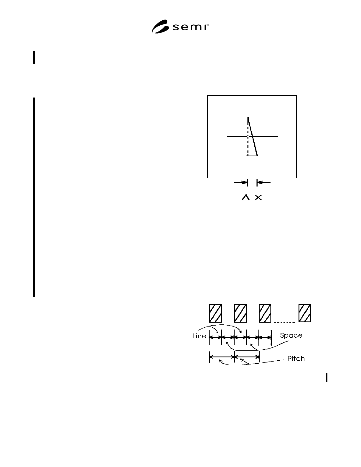
∆D = DM - DD
4.1.2 Rectangularity — Rectangular ity of array
pattern. Generally, it is indicated as deviation between
X coordinate 3 and 4 , when Y coordinate of 1 and 2 are
coincident.
3
21
4
Figure 1
Rectangularity
4.2 Overlay Accuracy — Deviatio n between two or
more masks in the direction of the long dimension X,
Y. Generally, the two methods are as follows:
• Deviation is measured by comparing the two
masks.
• Deviation is measured by comparing measured
data of each long dimension of the two masks.
4.3 Element Dimension Accuracy — Dimension
accuracy of element (line or space).
Figure 2
Element Dimension Accuracy
4.4 Repeat Pitch Accuracy — Deviation of measured
pitch length from designed value.
4.5 Stitching Error — Joint accura cy of a pattern
when a pattern is composed in a mask (e.g., pattern
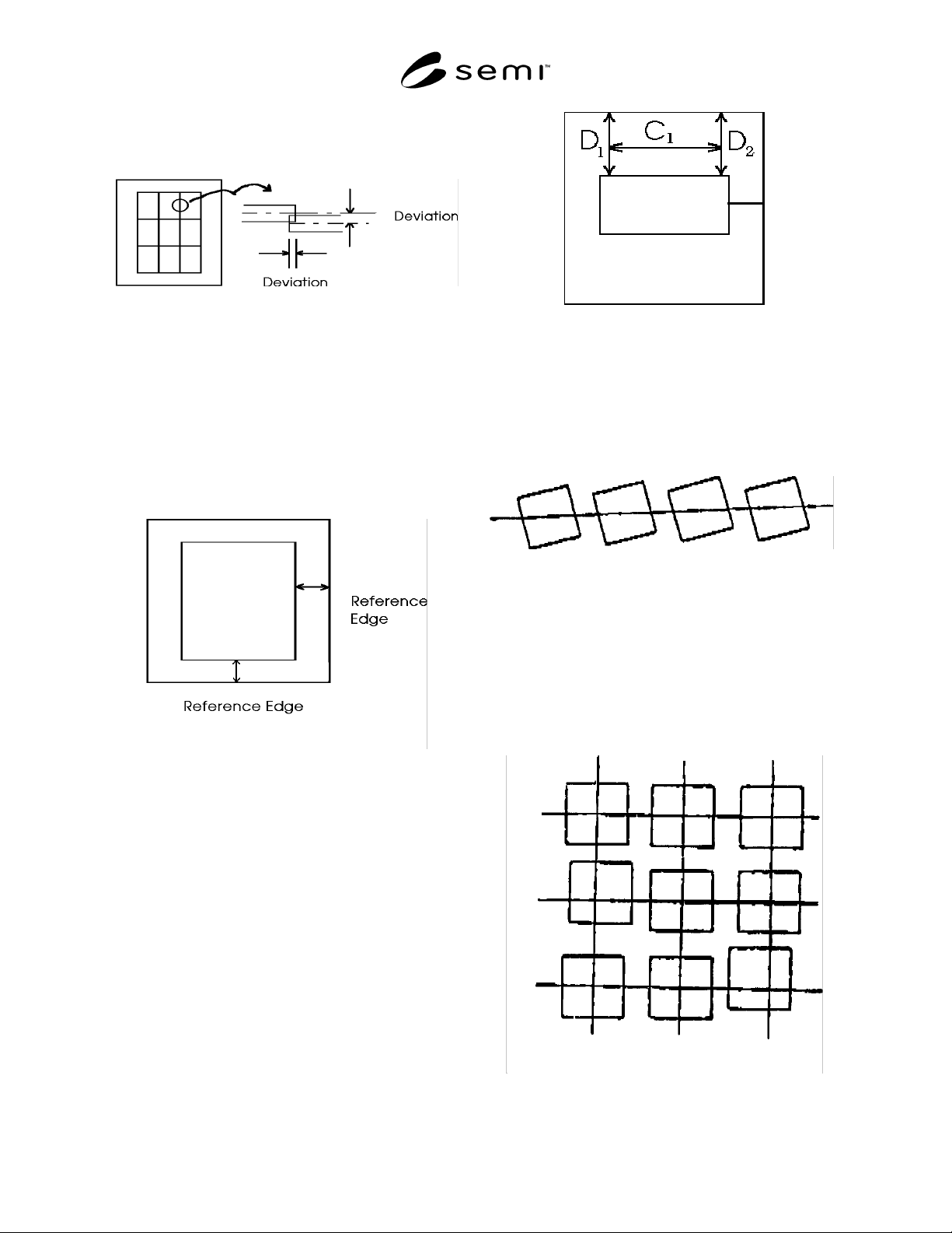
SEMI D21-1000 © SEMI 1992, 2000 2
composition by a stepper). Usually, it is deviation as
shown in the following figure.
Figure 3
Stitching Error
5 Pattern Positioning Accur acy
5.1 Pattern Positioning Accuracy — Relation between
the actual and desired locations of a printed pattern on a
glass substrate.
5.2 End Plane Reference — Positioning accuracy of
the printed pattern measured from the reference edge of
a glass mask.
Figure 4
Pattern Positioning Accuracy
5.2.1 Reference Edge: Two adjacent edges are
considered as the reference edge.
5.3 Pattern Rotation — Deviation of a printed pattern
on a glass mask caused by rotation. Usually, it is
expressed by the difference between two measured
distances at separated points within one side as shown
in the figure.
θ = (D
1
- D
2
)/C
1
Usually fix the value of C
1
and use the value of D
1
- D
2
.
Figure 5
Pattern Rotation
5.4 Cell Rotation in Multiimages — Cell’s slant
rotation against axis of light in case of exposure by
stepper and similar equipment. (Generally, it is
measured by vernier outside of cells.)
Figure 6
Cell Rotation in Multiimages
5.5 Gaps of Cells in Multiimages — X and Y
directions’ gaps of cells against designed grating which
should be exposed primarily by stepper and similar
equipment. (Generally, it is measured by gaps between
cells which are next to each other with vernier outside
of cells.)
Figure 7
Gaps of Cells in Multiimages