semi合集-English.pdf - 第561页
SEMI E78-1102 © SEMI 1998, 2002 19 Sparrow, E. M. and Geiger, G. T., “Local and Average Heat Transfer Characteris tics for a Disk Situated Perpendicular to a Uniform Plow”, J. He at Transfer 127: p. 32 1–326 (1985) Feder…
SEMI E78-1102 © SEMI 1998, 2002 18
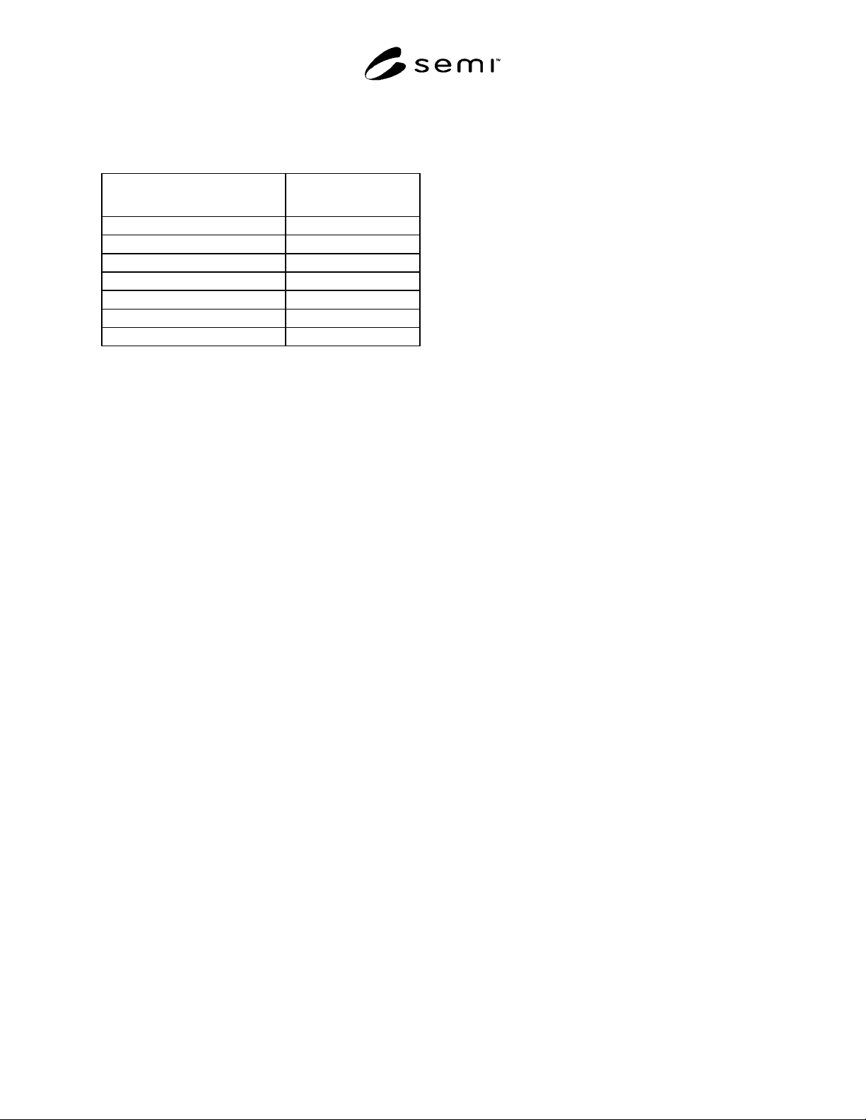
Table R1-2 Tolerable Levels of Electrostatic Field at
a Distance of One Radius from the Center of a
Wafer, Assuming a Fuchs Charge Distribution on
the Particles
Minimum Particle Diameter d in
µm
Tolerable Field E
0
, in
Volts/cm
0.01 15
0.02 21
0.03 26
0.05 34
0.10 47
0.20 67
0.30 82
R1-2.4 Conclusions — As indicated in Table R1-2, the
calculated value of tolerable electrostatic field (the
value of electrostatic field above which electrostatic
particle deposition becomes the dominant mechanism
of particle deposition) is just 47 V/cm for particles of
0.1 µm diameter when the particle electrical charge is
that described by the Fuchs charge distribution, a
minimum value of particle charge that is normally
exceeded in most environments. In most realistic
environments the particle charge will be greater and the
tolerable electrostatic field, even lower. Hence the
conclusion that in all practical processing environments
electrical forces will be the dominant mechanism of
particle deposition on wafers.
R1-2.4.1 In a Federal Standard 209E Class 1
environment (c ≤ 0.00124 particles/cm
3
) with v
elect
, ~
0.01 cm/s (the value predicted by Equation 10 for a 0.1
µm particle in an electric field of 47 Volts/cm) the
target areal particle densities (N/A = 0.016 particles/cm
2
for the 0.25 µm technology of 1998) specified in the
National Technology Roadmap for Semiconductors
(NTRS, 1994) will be reached after an exposure time of
about 1300 seconds, assuming c is at its maximum
allowed concentration.
R1-2.4.2 With less favorable electrical conditions, or
higher particle concentration, the maximum allowed
exposure time becomes shorter. In addition, the target
values for N/A continue to decrease with each
technology generation. Fortunately, one or more of the
parameters, particle concentration in the ambient, the
charge level on a surface, or the time a charged surface
is exposed to a given particle ambient, can be
controlled.
R1-2.4.3 Charge Neutralization — Achieving the
Fuchs charge distribution by means of radioactive
isotopes or balanced corona neutralizers — is the first
step in controlling particle deposition on wafers. This
step, while clearly necessary, is unlikely to be sufficient
to guarantee meeting the NTRS requirements of the
future. Steps to minimize environmental particle
concentration, c, and time of exposure, t, will have to be
part of the strategy for creating acceptable processing
environments. Minimizing these variables reduces
particle deposition attributable to all mechanisms, not
just electrostatic deposition.
R1-2.4.4 Contemporary standards recognize the need
for reduced particle concentrations in wafer
environments. For example, the classification ISO Class
1 (of the proposed international standard for classifying
cleanrooms according to concentration of airborne
particulate cleanliness) describes an environment in
which the concentration of particles > 0.1 µm is 10
-5
particles/cm
3
or less. In an environment of this quality,
wafer exposure can be as long as 10
5
seconds at the
deposition velocity predicted for neutralized 0.1 µm
particles (~0.01 cm/s) and still meet the target defect
density that the NTRS recommends for the 0.1 µm
technology anticipated in 2007. Fractional increases in
the electric field above 47 Volts/cm will decrease the
allowed exposure time by that same fraction (Equations
10, 12) — an electric field of 94 Volts/cm reduces the
allowed exposure time to 5 × 10
4
seconds, etc.
R1-2.5 References
Bae, G.N., Lee, C. S., and Park, S. O., “Measurement of
Particle Deposition Velocity Toward a Horizontal
Semiconductor Wafer by Using a Wafer Surface
Scanner”, Aerosol Science Technology 21: p. 72–82
(1994)
Cooper, D. W., Miller, R. J., Wu, J. J., and Peters, M.
H., “Deposition of Submicron Aerosol Particles During
Integrated Circuit Manufacturing: Theory”, Particulate
Science Technology 8 (3 and 4): p. 209–224 (1990)
Fuchs, N. A., The Mechanics of Aerosols, Pergamon
Press, Oxford (1964)
Liu, B. Y. H., and Ahn, K. H., “Particle Deposition on
Semiconductor Wafers”, Aerosol Science Technology 6:
p. 215–224 (1987)
National Technology Roadmap for Semiconductors,
Semiconductor Industry Association, 4300 Stevens
Creek Boulevard, Suite 271, San Jose, CA 95129, 1994
Oh, M. D., Yoo, K. H., and Myong, H. K., “Numerical
Analysis of Particle Deposition onto Horizontal
Freestanding Wafer Surfaces Heated or Cooled”,
Aerosol Science Technology 25: p. 141–156 (1996)
Peters, M. H., and Cooper, D. W., “Approximate
Analytical Solutions for Particle Deposition in Viscous
Stagnation-Point Flow in the Inertial-Diffusion Regime
with External Forces”, J. Colloid Interface Science
142(1): p. 140–148 (1991)

SEMI E78-1102 © SEMI 1998, 2002 19
Sparrow, E. M. and Geiger, G. T., “Local and Average
Heat Transfer Characteristics for a Disk Situated
Perpendicular to a Uniform Plow”, J. Heat Transfer
127: p. 321–326 (1985)
Federal Standard 209E — “Airborne Particulate
Cleanliness Classes in Cleanrooms and Clean Zones”
R1-2.6 Experimental Reference
R1-2.6.1 Deposition of 0.1 to 1.0 Micron Particles,
Including Electrostatic Effects, onto Silicon Monitor
Wafers (Experimental)
R1-2.6.2 William J. Fosnight, Vaughn P. Gross,
Kenneth D. Murray, Richard D. Wang, IBM
Corporation published in 1993 Microcontamination
Conference proceedings
R1-2.6.3 Summary: Submicron particle contamination
continues to be a concern in the manufacture of
integrated circuits. Quantifying particle deposition
velocity (the ratio of particle deposition rate to airborne
particle concentration) is of fundamental importance in
understanding the defect-density impact of airborne
contamination.
R1.2.6.4 As particle size decreases, the effect of
electrostatic charge plays an increasing role in the
deposition of particles onto surfaces. This four-trial
study examines the deposition of 0.1 to 1.0 micron
particles onto horizontal, grounded and electrostatically
charged, silicon monitor wafers in an 80 feet per minute
vertical unidirectional airflow. The experimental
deposition velocity results were compared to theoretical
predictions found in the literature.
R1-2.6.5 Three primary observations were obtained
from this study. First, measured values of deposition
velocity agreed reasonably well with predicted values.
However, deposition velocity was not observed to
increase below 0.2 micron. Secondly, particles less than
0.5 micron were observed to deposit onto charged
wafers approximately three to ten times faster than onto
grounded (not charged) wafers. Finally, settling monitor
wafers may be a time consuming (and expensive)
means of certifying the cleanliness of a “clean” (less
than 10 ppcf at scanner threshold particle size)
environment. However, settling-monitor studies should
not be confused with particles-per-wafer-pass (PWP)
measurements; PWP measurements often provide
useful information regarding the performance of the
automation and/or process of a tool, even if it is in a
very clean environment.
R1-3 ESD Impacts in Semiconductor
Equipment
Contributed by Julian A. Montoya, Intel Corporation,
5200 NE Elam Young Parkway, Hillsboro OR, 97124-
6497.
R1-3.1 Introduction — Electrostatic phenomena impact
semiconductor manufacturing in many ways. These
range from increased particle accumulation on wafer
surfaces to electrostatic discharge (ESD) events which
impact equipment performance, and in some cases
impact factory yields and throughput.
R1-3.1.1 All areas within a semiconductor
manufacturing environment must be concerned with
electrostatic control. This encompasses initial wafer
receiving to shipping of final product. In addition, the
equipment which will be housed within that
environment must also be concerned with electrostatic
control and electrostatic immunity.
R1-3.1.2 This section highlights issues associated with
static charge and ESD in a semiconductor
manufacturing environment and its effects on
production equipment.
R1-3.2 Overview — Static charge issues in
semiconductor manufacturing manifest themselves in
many ways. Problems occur by direct contact with
charged items, by induction from electrostatic fields,
and indirectly by radiated and conducted
electromagnetic interference (EMI) emitted into the
environment as a result of the ESD event.
R1-3.3 Equipment ESD Examples — The following
section presents real world examples of the cause and
impacts associated with electrostatic discharge and
semiconductor manufacturing equipment.
R1-3.3.1 Charged operators came into direct contact
with diffusion furnace control panel. Process aborted on
many occasions resulting in loss of product and reduced
equipment utilization.
R1-3.3.2 Numerous instances where charged reticles
(photomasks) came into direct contact with a grounded
object. This caused damage to reticles and impacted
factory throughput. Costs were associated with
replacing damaged reticles and requalifying reticle sets.
R1-3.3.3 Charged operators came into direct contact
with electronic card cage of chemical vapor deposition
tool. This resulted in process abort, loss of product, and
reduced equipment availability.
R1-3.3.4 Charged wafer cassette induced charge onto
robot arm on wafer transfer tool. Robot arm came into
contact with grounded screw creating an ESD event.
This resulted in data corruption which caused robot

SEMI E78-1102 © SEMI 1998, 2002 20
arms to open, dropping fully loaded wafer cassettes to
the floor. Costs were associated with loss of product.
R1-3.3.5 Automated material handling system “car”
became charged while coming in close proximity to
ionizer. Car came into contact with grounded object
during charging; creating data corruption which
resulted in system downtime, impact to factory
throughput, and cost associated with the replacement of
control electronics.
R1-3.3.6 Wafer taping/detaping tool generated charge
during normal operation. Chassis ground of the tool
was inadvertently removed, causing high charge to be
developed within the tool. Electrostatic Discharge
occurred at random time intervals within the tool.
Impact to equipment availability, and long solution
time.
R1-3.3.7 Wafers became charged during spin rinse
process. During transfer to wafer metrology tool
electrostatic discharge occurred, causing data
corruption. This resulted in unexpected tool lockups,
and reduced equipment availability.
R1-3.3.8 Ungrounded wall panels became charged and
generated ESD events. EMI produced from ESD events
coupled into photolithography equipment and created
data corruption. This resulted in impacts to equipment
utilization. Long solution time.
R1-3.3.9 Insulative ceiling panels became charged and
generated ESD events which produced high levels of
radiated and conducted EMI in a test area. EMI coupled
into tester/handler and produced data scramble. This
resulted in reduced equipment availability.
R1-3.3.10 Finished product became charged during
manual handling. Product came into direct contact with
test/handler equipment. This resulted in damaged
circuit cards which needed to be replaced, and
decreased equipment availability.
R1-3.3.11 Wafer transfer cart became charged while
rolling over temporary “insulative” floor. Cart came
into contact with plasma etcher control cabinet.
Resulting ESD event caused product loss and reduced
equipment availability.
R1-3.3.12 Wafer polisher robot arm became charged
during normal operation. Chassis ground wire for robot
left off. ESD event occurred causing data scramble
which resulted in process being aborted.
R1-3.4 Conclusion — Electrostatic Discharge (ESD)
affects semiconductor manufacturing equipment in
many ways. The issues are wide ranging from trivial
lock-ups and aborts of process equipment to factory
throughput and yields impacts. The scope of the ESD
problem is very broad and encompasses every aspect of
semiconductor manufacturing.