semi合集-English.pdf - 第7609页
SEMI T1-95 © SEMI 1993, 2003 10 Figure R1-1 Code Field Locations for Flatted Wafers (See Tables R1-1 and 5.) Figure R1-2 Code Field Locations for Notched Wafers (See Tables R1-2 and 5.) NOTICE: SEMI makes no warranties o…
SEMI T1-95 © SEMI 1993, 2003 9
RELATED INFORMATION 1
APPLICATION NOTES
NOTICE: This related information section is not an official part of SEMI T1 and is not intended to modify or supercede the
official standard. Rather, this note is provided primarily as a source of information to aid in the application of the standard. As
such, it is considered reference material only. The standard should be referred to in all cases.
R1-1 Center Reference Dimensions for Bar
Code and Optional Alphanumeric Marks
R1-1.1 The following information is provided as a
reference for equipment which employs center
referencing to locate the bar code or optional
alphanumeric marks. Dimensions for flatted wafers are
given in Table R1-1 and dimensions for notched wafers
are given in Table R1-2.
R1-2 Referenced Documents
R1-2.1 SEMI Standards
SEMI M1.7 — Standard for 125 mm Polished Mono-
crystalline Silicon Wafers
SEMI M1.8 — Standard for 150 mm Polished Mono-
crystalline Silicon Wafers
SEMI M1.9 — Standard for 200 mm Polished Mono-
crystalline Silicon Wafers (Notched)
SEMI M1.10 — Standard for 200 mm Polished Mono-
crystalline Silicon Wafers (Flatted)
SEMI M1.12 — Standard for 125 mm Polished Mono-
crystalline Silicon Wafers Without Secondary Flat
SEMI M1.13 — Standard for 150 mm Polished Mono-
crystalline Silicon Wafers Without Secondary Flat (625
µm Thickness)
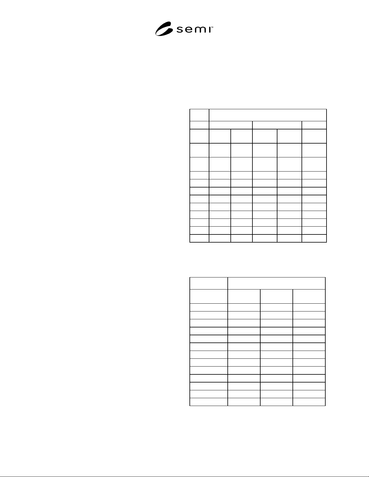
Table R1-1 Mark Distances on Flatted Wafers
(see Figure R1-1)
Wafer Size and SEMI Standards
125 mm 150 mm 200 mm
Dim. in
mm
SEMI
M1.7
SEMI
M1.12
SEMI
M1.13
SEMI
M1.8
SEMI
M1.10
D 125 ±
0.5
125 ±
0.2
150 ± 0.2 150 ± 0.2 200 ± 0.2
FL 42.5 ±
2.5
475. ±
2.5
47.50 ±
2.5
57.50 ±
2.5
57.50 ±
2.5
Znom 58.83 58.83 71.19 69.32 95.83
Zmax 59.53 59.37 71.70 69.93 96.30
Zmin 58.09 58.25 70.66 68.68 95.34
R1nom 54.48 54.48 66.84 64.97 91.48
R1max 55.59 55.53 67.86 66.10 92.46
R1min 53.23 53.39 65.79 63.82 90.08
K1nom 1.03 1.03 1.03 1.03 1.03
K1max 1.55 1.55 1.55 1.55 1.55
K1min 0.05 0.50 0.50 0.50 0.50
D = Wafer Diameter
FL = Primary Flat Length
Table R1-2 Mark Distances on Notched Wafers
(see Figure R1-2)
Wafer Size and SEMI Standards
Dim. in mm 125 mm 150 mm 200 mm
SEMI M1.9
D 125 ± 0.5 150 ± 0.2 200 ± 0.2
Z1nom 0.80 0.80 0.80
Z1max 1.05 1.05 1.05
Z1min 0.30 0.30 0.30
R1nom 54.90 67.40 92.40
R1max 55.91 68.26 93.26
R1min 53.64 66.29 91.29
K1mon 3.28 3.28 3.28
K1max 4.05 4.05 4.05
K1min 2.50 2.50 2.50
Ynom 1.80 1.80 1.80
Y1max 2.05 2.05 2.05
Y1min 1.55 1.55 1.55
D = Wafer Diameter
SEMI T1-95 © SEMI 1993, 2003 10
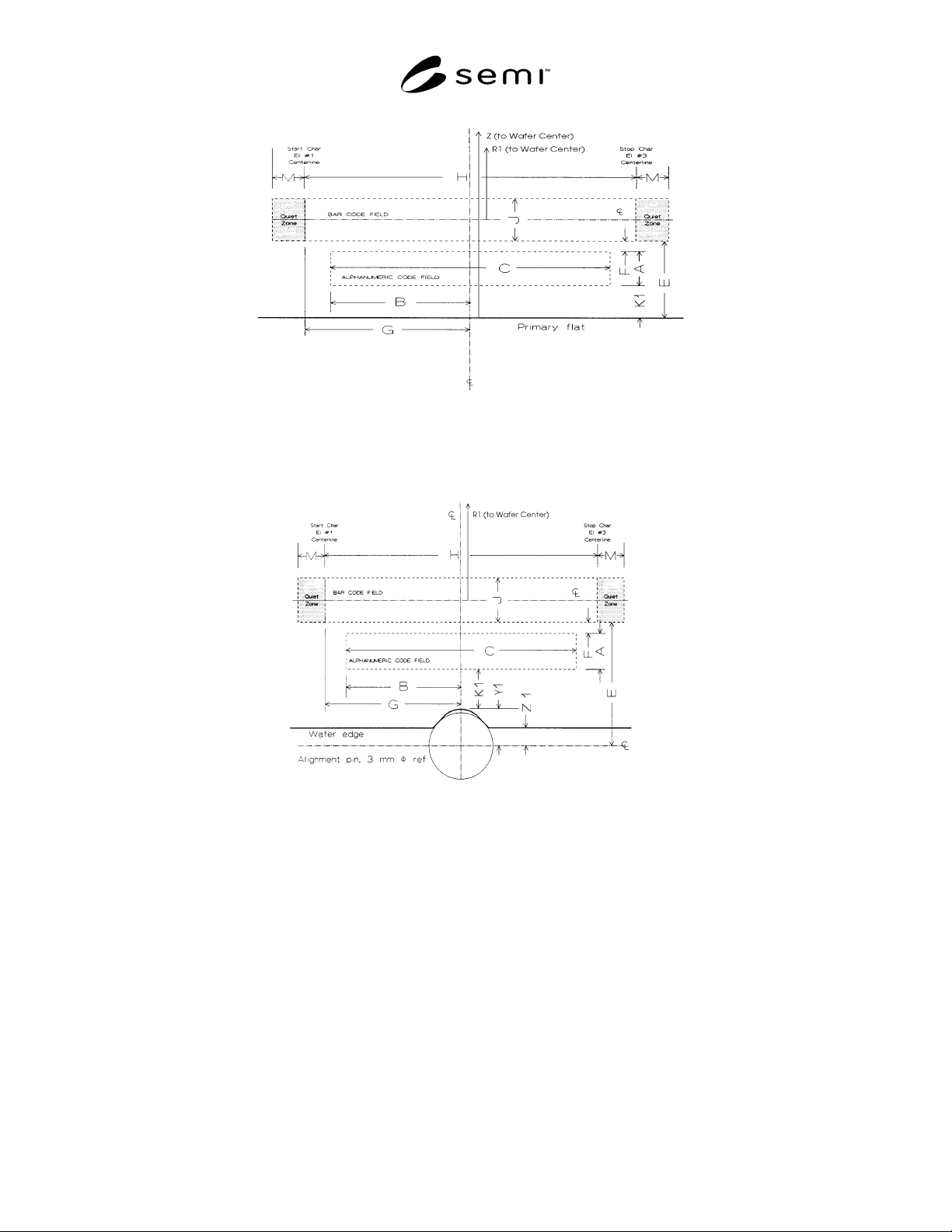
Figure R1-1
Code Field Locations for Flatted Wafers (See Tables R1-1 and 5.)
Figure R1-2
Code Field Locations for Notched Wafers (See Tables R1-2 and 5.)
NOTICE: SEMI makes no warranties or representations as to the suitability of the standards set forth herein for any
particular application. The determination of the suitability of the standard is solely the responsibility of the user.
Users are cautioned to refer to manufacturer's instructions, product labels, product data sheets, and other relevant
literature, respecting any materials or equipment mentioned herein. These standards are subject to change without
notice.
By publication of this standard, Semiconductor Equipment and Materials International (SEMI) takes no position
respecting the validity of any patent rights or copyrights asserted in connection with any items mentioned in this
standard. Users of this standard are expressly advised that determination of any such patent rights or copyrights, and
the risk of infringement of such rights are entirely their own responsibility.
Copyright by SEMI® (Semiconductor Equipment and Materials
International), 3081 Zanker Road, San Jose, CA 95134. Reproduction o
f
the contents in whole or in part is forbidden without express written
consent of SEMI.
SEMI T2-0298
(Reapproved 1104)
SPECIFICATION FOR MARKING OF WAFERS WITH A TWO-
DIMENSIONAL MATRIX CODE SYMBOL
This specification was technically approved by the Global Traceability Committee and is the direct
responsibility of the North American Traceability Committee. Current edition approved by the North
American Traceability Committee on July 11, 2004. Initially available at www.semi.org September 2004; to
be published November 2004. Originally published in 1993; last published February 1998.
1 Purpose
1.1 This specification is intended to provide a marking
symbology that can be used to mark silicon wafers with
minimum intrusion into the fixed quality area of the
wafer.
2 Scope
2.1 This specification defines the geometric and spa-
tial relationships and content (including the error check-
ing and correcting code) of a two-dimensional (2-D),
machine-readable, binary matrix code symbol for front
surface marking of wafers of silicon which comply with
SEMI M1, SEMI M2, or SEMI M11, and other mater-
ials with diameters of 125 to 200 mm. This specifica-
tion allows for consistency of all wafer marking per-
formed by wafer manufacturers. It may be used in con-
junction with, or as an alternative to, the alphanumeric
marking codes specified in SEMI M12 and SEMI M13
or a front surface bar code like that specified in SEMI
T1.
2.2 Although this specification does not specify the
marking techniques that may be employed when com-
plying with its requirements, it is assumed that the sym-
bol will be obtained by laser scribing individual dots.
2.3 The 2-D matrix code is applicable to a broad range
of wafer products, including epitaxial wafers, SOI wa-
fers, and unpatterned or patterned polished wafers. The
format and algorithms of this code are based on the Da-
ta Matrix two-dimensional symbology specified in AIM
International Symbology Specification - Data Matrix.
NOTICE: This standard does not purport to address
safety issues, if any, associated with its use. It is the
responsibility of the users of this standard to establish
appropriate safety and health practices and determine
the applicability of regulatory or other limitations prior
to use.
3 Referenced Standards
3.1 SEMI Standards
SEMI AUX001 — List of Vendor Identification Codes
SEMI M1 — Specifications for Polished Monocrys-
talline Silicon Wafers
SEMI M2 — Specification for Silicon Epitaxial Wafers
for Discrete Device Applications
SEMI M11 — Specifications for Silicon Epitaxial
Wafers for Integrated Circuit (IC) Applications
SEMI M12 — Specification for Serial Alphanumeric
Marking of the Front Surface of Wafers
SEMI M13 — Specification for Alphanumeric Marking
of Silicon Wafers
SEMI T1 — Specification for Back Surface Bar Code
Marking of Silicon Wafers
3.2 AIM International Technical Specification
1
AIM International Symbology Specification - Data
Matrix
3.3 ANSI Standard
2
ANSI X3.4 — American Standard Code for
Information Interchange (ASCII)
NOTE 1: This standard is equivalent to ISO 646, Information
Processing - ISO 7-bit Coded Character Set for Information
Processing.
NOTICE: Unless otherwise indicated, all documents
cited shall be the latest published versions.
1 AIM International Inc., 125 Warrendale-Bayne Road, Warrendale,
PA 15086, +1 724 934 4470, Fax: +1 724 934 4495,
http://www.aimglobal.org/
2 American National Standards Institute, Headquarters: 1819 L
Street, NW, Washington, DC 20036, USA. Telephone: 202.293.8020;
Fax: 202.293.9287, New York Office: 11 West 42nd Street, New
York, NY 10036, USA. Telephone: 212.642.4900; Fax: 212.398.002,
Website: www.ansi.org
SEMI T2-0298 © SEMI 1993, 2004 1