semi合集-English.pdf - 第4840页
SEMI M1-0305 © SEMI 1978, 2005 16 ITEM SPECIFICATION MEASUREMENT METHOD 2-8.8 Edge Cracks [ ]None; [ ]Other: (specif y )___________ [ ]SEMI MF523; [ ]JIS H 0614; [ ]SSIS; #4 [ ]Other: (specify)___________ 2-8.9 Crack…
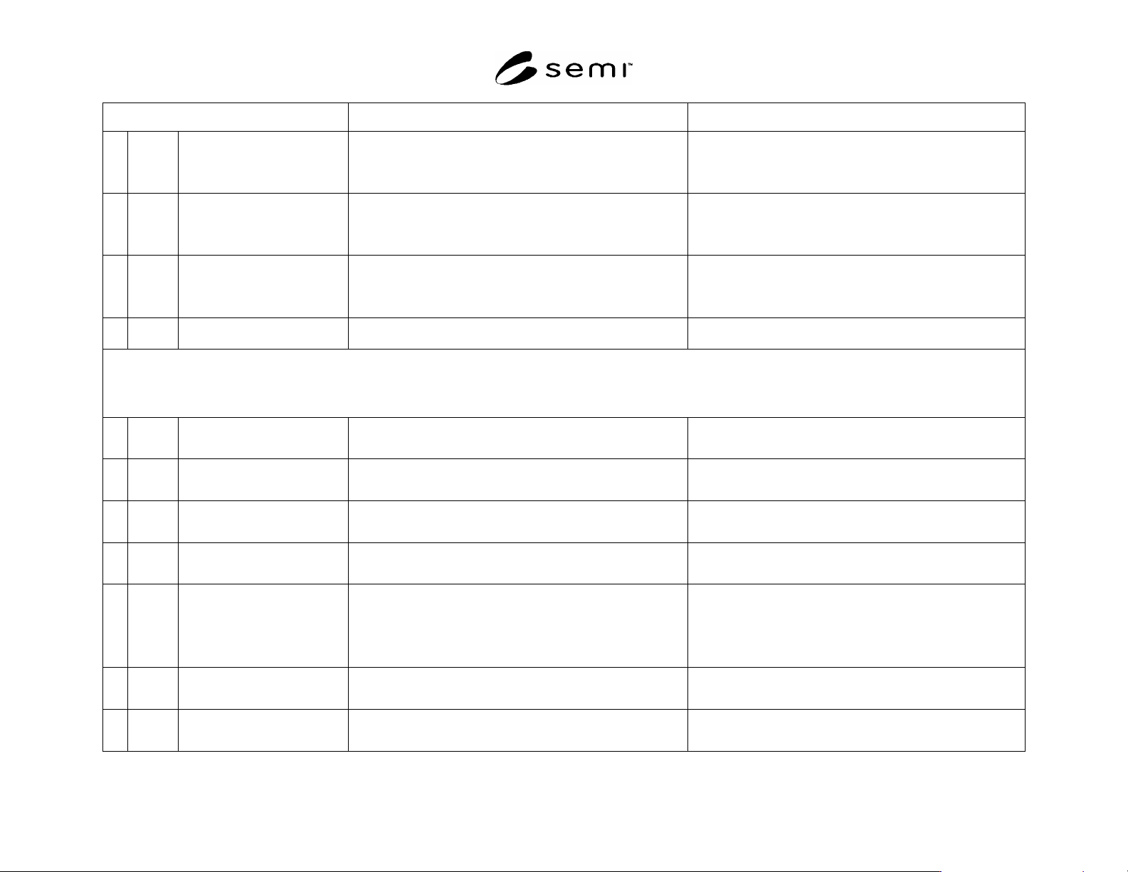
SEMI M1-0305 © SEMI 1978, 2005 15
ITEM SPECIFICATION MEASUREMENT METHOD
2-7.2.4 __________
[ ]Not greater than [ 10 ]atoms/cm
2
[ ]ICP/MS; [ ]AAS; [ ]SEMI MF1617 (SIMS);
[ ]SEMI M33 (TXRF);[ ]ISO 14706 (TXRF);
[ ]Other: (specify)_____________
2-7.2.5 __________
[ ]Not greater than [ 10 ]atoms/cm
2
[ ]ICP/MS; [ ]AAS; [ ]SEMI MF1617 (SIMS);
[ ]SEMI M33 (TXRF);[ ]ISO 14706 (TXRF);
[ ]Other: (specify)_____________
2-7.2.6 __________
[ ]Not greater than [ 10 ]atoms/cm
2
[ ]ICP/MS; [ ]AAS; [ ]SEMI MF1617 (SIMS);
[ ]SEMI M33 (TXRF);[ ]ISO 14706 (TXRF);
[ ]Other: (specify)_____________
2-7.3 Surface Organics [ ]Not greater than [ ]ng/cm
2
[ ]SEMI MF1982; [ ]Other: (specify)___________
2-8. FRONT SURFACE INSPECTION CHARACTERISTICS
FOR ALL WAFER DIAMETERS, THE ITEMS LISTED IN THIS SECTION MAY BE SPECIFIED INDIVIDUALLY. ALTERNATIVELY, FOR WAFERS
150 mm OR LESS IN DIAMETER, WHICH CAN BE INSPECTED VISUALLY, THE ITEMS LISTED MAY BE [ ]Specified according to Table 10. If the
items are specified according to Table 10, the items marked with the symbol need not be entered individually.
2-8.1 Scratches – Macro
[ ]None; [ ]Other: (specify)___________ [ ]SEMI MF523; [ ]JIS H 0614; [ ]SSIS;
#4
[ ]Other: (specify)___________
2-8.2 Scratches – Micro [ ]None; [ ]Other: (specify)___________ [ ]SEMI MF523; [ ]JIS H 0614; [ ]SSIS;
#4
[ ]Other: (specify)___________
2-8.3 Pits
[ ]None; [ ]Other: (specify)___________ [ ]SEMI MF523; [ ]JIS H 0614; [ ]SSIS;
#4
[ ]Other: (specify)___________
2-8.4 Haze
[ ]None; [ ]Other: (specify)___________ [ ]SEMI MF523; [ ]JIS H 0614; [ ]SSIS;
#4
[ ]Other: (specify)___________
2-8.5 Localized Light Scatterers
(LLS)
Size: [ ] m (LSE) Count: [ ] [ ] per wafer; [ ] per cm
2
Size: [ ] m (LSE) Count: [ ] [ ] per wafer; [ ] per cm
2
Size: [ ] m (LSE) Count: [ ] [ ] per wafer; [ ] per cm
2
Size: [ ] m (LSE) Count: [ ] [ ] per wafer; [ ] per cm
2
Size: [ ] m (LSE) Count: [ ] [ ] per wafer; [ ] per cm
2
[ ]SEMI MF523; [ ]JIS H 0614; [ ]SSIS;
#4
[ ]Other: (specify)___________
2-8.6 Contamination/Area
[ ]None; [ ]Other: (specify)___________
[ ]SEMI MF523; [ ]JIS H 0614; [ ]SSIS;
#4
[ ]Other: (specify)___________
2-8.7 Edge Chips and Indents
[ ]None; [ ]Other: (specify)___________
[ ]SEMI MF523; [ ]JIS H 0614; [ ]SSIS;
#4
[ ]Other: (specify)___________
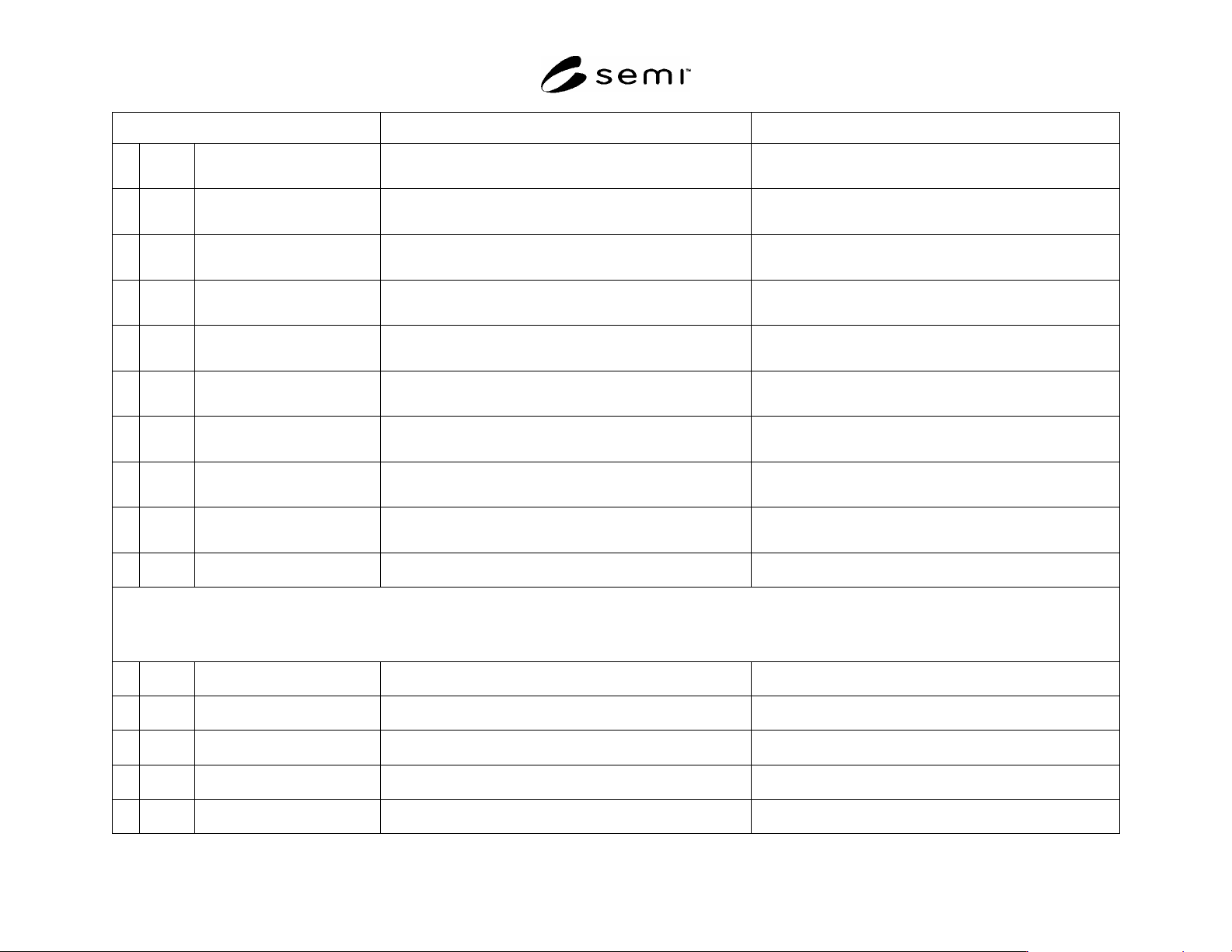
SEMI M1-0305 © SEMI 1978, 2005 16
ITEM SPECIFICATION MEASUREMENT METHOD
2-8.8 Edge Cracks
[ ]None; [ ]Other: (specify)___________
[ ]SEMI MF523; [ ]JIS H 0614; [ ]SSIS;
#4
[ ]Other: (specify)___________
2-8.9 Cracks, Crow’s Feet
[ ]None; [ ]Other: (specify)___________
[ ]SEMI MF523; [ ]JIS H 0614; [ ]SSIS;
#4
[ ]Other: (specify)___________
2-8.10 Craters
[ ]None; [ ]Other: (specify)___________
[ ]SEMI MF523; [ ]JIS H 0614; [ ]SSIS;
#4
[ ]Other: (specify)___________
2-8.11 Dimples
[ ]None; [ ]Other: (specify)___________ [ ]SEMI MF523; [ ]JIS H 0614; [ ]SSIS;
#4
[ ]Other: (specify)___________
2-8.12 Grooves
[ ]None; [ ]Other: (specify)___________ [ ]SEMI MF523; [ ]JIS H 0614; [ ]SSIS;
#4
[ ]Other: (specify)___________
2-8.13 Mounds
[ ]None; [ ]Other: (specify)___________ [ ]SEMI MF523; [ ]JIS H 0614; [ ]SSIS;
#4
[ ]Other: (specify)___________
2-8.14 Orange Peel
[ ]None; [ ]Other: (specify)___________ [ ]SEMI MF523; [ ]JIS H 0614; [ ]SSIS;
#4
[ ]Other: (specify)___________
2-8.15 Saw Marks
[ ]None; [ ]Other: (specify)___________ [ ]SEMI MF523; [ ]JIS H 0614; [ ]SSIS;
#4
[ ]Other: (specify)___________
2-8.16 Dopant Striation Rings [ ]None; [ ] Other: (specify)______________________ [ ]SEMI MF523; [ ]JIS H 0614; [ ]DIN 50443/1;
[ ]Other: (specify)___________
2-8.17 Stains
[ ]None; [ ] Other: (specify)______________________
[ ]SEMI MF523; [ ]JIS H 0614; [ ]Other: (specify)___________
2-9. BACK SURFACE INSPECTION CHARACTERISTICS
FOR ALL WAFER DIAMETERS, THE ITEMS LISTED IN THIS SECTION MAY BE SPECIFIED INDIVIDUALLY. ALTERNATIVELY, FOR WAFERS
150 mm OR LESS IN DIAMETER, WHICH CAN BE INSPECTED VISUALLY, THE ITEMS LISTED MAY BE [ ]Specified according to Table 10. If the
items are specified according to Table 10, the items marked with the symbol need not be entered individually.
2-9.1 Edge Chips
[ ]None; [ ]Other: (specify)___________ [ ]SEMI MF 523; [ ]JIS H 0614; [ ]Other: (specify)__________
2-9.2 Edge Cracks [ ]None; [ ]Other (specify)______________ [ ]SEMI MF 523; [ ]JIS H 0614; [ ]Other: (specify)__________
2-9.3 Cracks, Crow’s Feet
[ ]None; [ ]Other: (specify)___________ [ ]SEMI MF 523; [ ]JIS H 0614; [ ]Other: (specify)__________
2-9.4 Contamination/Area
[ ]None; [ ]Other: (specify)___________ [ ]SEMI MF 523; [ ]JIS H 0614; [ ]Other: (specify)__________
2-9.5 Saw Marks
[ ]None; [ ]Other: (specify)___________ [ ]SEMI MF 523; [ ]JIS H 0614; [ ]Other: (specify)__________
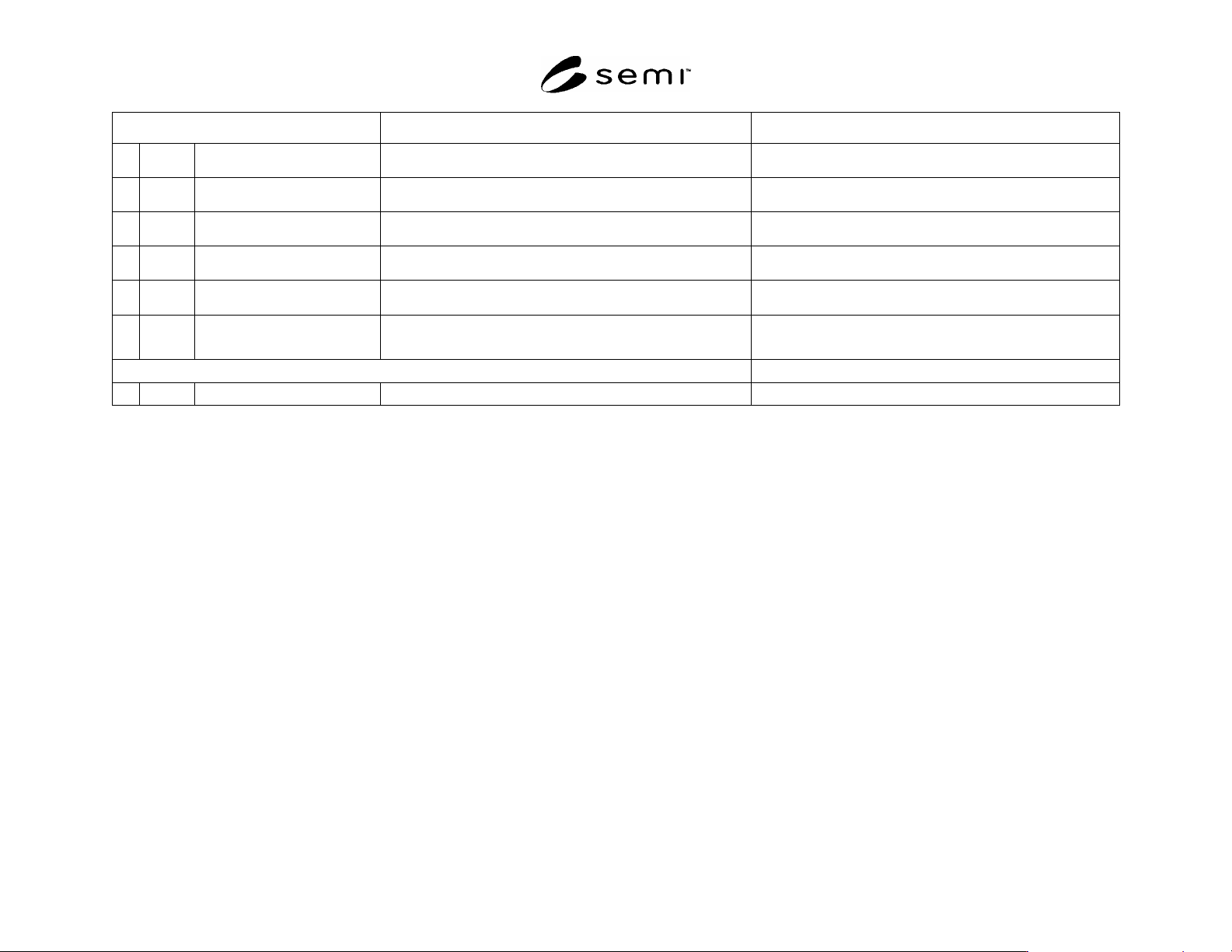
SEMI M1-0305 © SEMI 1978, 2005 17
ITEM SPECIFICATION MEASUREMENT METHOD
2-9.6 Stains [ ]None; [ ] Other: (specify)______________________ [ ]SEMI MF 523; [ ]JIS H 0614; [ ]Other: (specify)__________
2-9.7 Roughness [ ] ________ nm rms [ ] SEMI M40; [ ]Other: (specify)______________
2-9.8 Brightness (Gloss) [ ] ______________________ [ ]ASTM D 523; [ ]JIS Z 8741; [ ]Other: (specify)___________
2-9.9 Scratches – Macro [ ]None; [ ]Cum Length =[ ]mm [ ]SEMI MF 523; [ ]JIS H 0614; [ ]Other: (specify)__________
2-9.10 Scratches – Micro [ ]None; [ ]Cum Length =[ ]mm [ ]SEMI MF 523; [ ]JIS H 0614; [ ]Other: (specify)__________
2-9.11 Localized Light Scatterers
Size: [ ] m (LSE) Count: [ ] [ ] per wafer; [ ] per cm
2
Size: [ ] m (LSE) Count: [ ] [ ] per wafer; [ ] per cm
2
[ ]SEMI MF 523; [ ]JIS H 0614; [ ]SSIS
#4
;
[ ]Other: (specify)____
2-10. OTHER (as required)
#1
The nominal edge exclusion, EE, specifies the diameter of the FQA, which is given by the nominal diameter (see Item 2-6.1) minus 2EE (see Figure 1). This quantity provides a center referenced
property. Although use of edge referenced properties is discouraged, some equipments and procedures are based on edge referenced dimensions. When this occurs, the quality area is not fixed and
some part of the fixed quality area may fall outside the evaluated area, which is generally not a desirable situation.
#2
If specified as polished, this term is meant to imply a surface condition and not a particular processing technique. If desired, a quantitative measure of surface finish may optionally be indicated by
specifying the rms microroughness over a specified spatial frequency (or wavelength) range. Because a standardized test method has not yet been developed for this metric, both values and test
procedures, including sampling plan and detrending procedures, shall be agreed upon between supplier and customer.
#3
Flatness Acronyms are defined in the Flatness Decision Tree in Appendix 1.
#4
In today’s technology, it may be possible to inspect for some of these items using automated surface scanning inspection systems (SSIS). Such systems should be calibrated according to SEMI M53
using polystyrene latex spheres deposited in accordance with SEMI M58. Some indication of the defects separable by such instruments is provided in SEMI M35; however, a standard test procedure has
yet to be developed. Application of automated inspection with the use of an SSIS must be agreed upon between supplier and customer.