semi合集-English.pdf - 第34页
SEMI E1.9-0701 E2 © SEMI 1994, 2004 14 Table 1 Cassette Dime nsions Symbol Used Figure Number Value Specified Datum Measured from Boundary or Feature Measured to ω 13 0° minimum 2° maximum horizontal datum plane fork-lif…
SEMI E1.9-0701
E2
© SEMI 1994, 2004 13
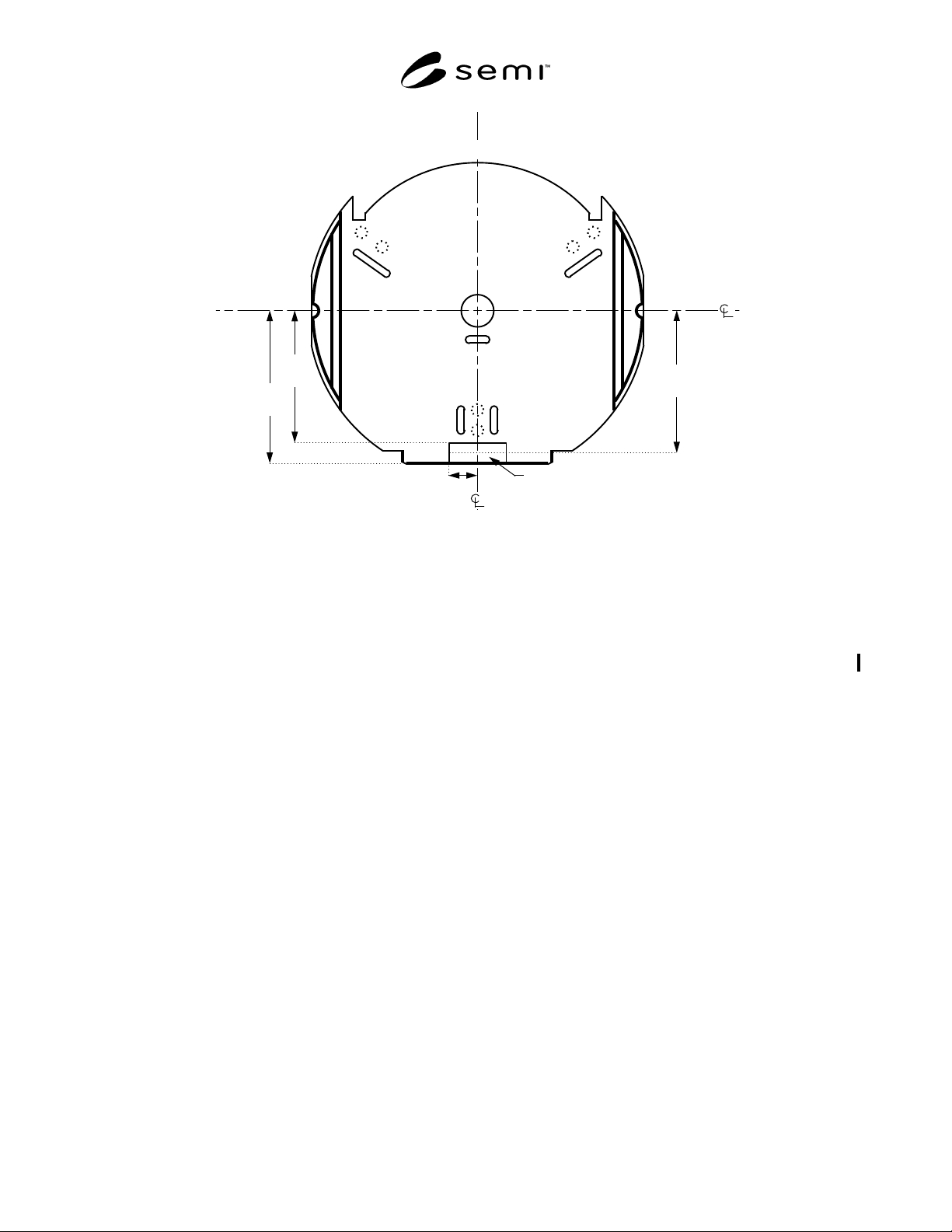
x25 ≥30
y16
=155 ±1
y24
≤136
cassette
identification
tag area
front side of the cassette where wafers are accessed
facial
datum
plane
bilateral datum plane
y22
=145
Figure 16
Optional Bottom Cassette Identification Tag Area
6.9 Pitch and Capacity — Table 2 shows the different
options with regard to the wafer pitch (spacing) and the
cassette capacity. Again, no tolerance is given on the
wafer pitch (z12), for reasons given in Section 6.7.
6.10 Inner and Outer Radii — All concave features
may have a radius no greater than r15 to allow cleaning
and to prevent contaminant build-up. All required
convex features must also have a radius of r16 to
prevent small contact patches with large stresses that
might cause wear and particles. Here a required feature
is an area on the surface of the carrier specified by a
dimension (or intersections of dimensions) that has a
tolerance and not just a maximum or minimum (such as
the rim of the fork-lift pin hole, the edges of the robotic
handling flanges, and the corners at the rear of the
cassette top and bottom domains).
6.11 Vertical Wafer Access — This standard does not
cover accessing wafers in a vertical orientation.
7 Related Documents
7.1 SEMI Standards
SEMI E22.1 — Cluster Tool Module Interface
300 mm: Transport Module End Effector Exclusion
Volume Standard
SEMI E47.1 — Provisional Mechanical Specification
for Boxes and Pods Used to Transport and Store 300
mm Wafers
SEMI E62 — Provisional Specification for 300 mm
Front-Opening Interface Mechanical Standard (FIMS)
SEMI E63 — Provisional Mechanical Specification for
300 mm Box Opener/Loader to Tool Standard
(BOLTS-M) Interface
SEMI E103 — Provisional Mechanical Specification
for a 300 mm Single-Wafer Box System that Emulates
a FOUP
SEMI M28 — Specification for Developmental 300
mm Diameter Polished Single Crystal Silicon Wafers
SEMI M31 — Provisional Mechanical Specification for
Front-Opening Shipping Box Used to Transport and
Ship 300 mm Wafers
SEMI E1.9-0701
E2
© SEMI 1994, 2004 14
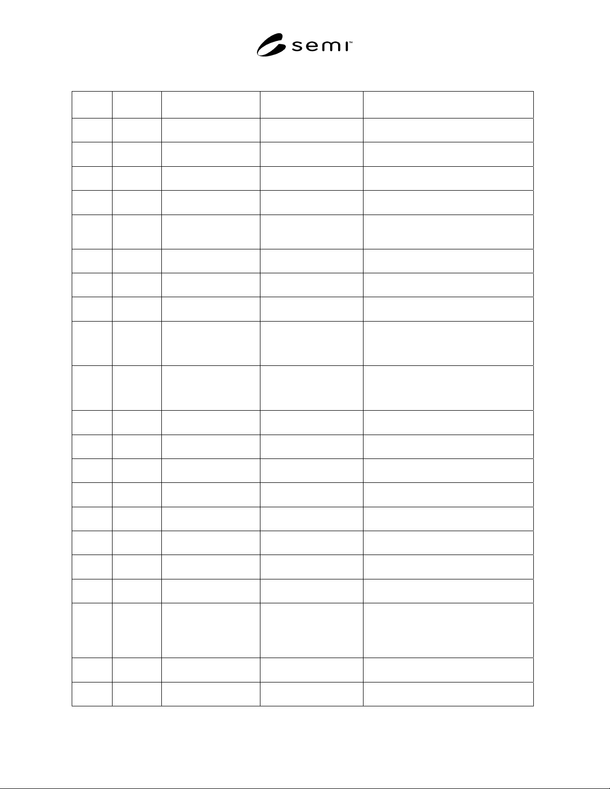
Table 1 Cassette Dimensions
Symbol
Used
Figure
Number
Value Specified Datum Measured from Boundary or Feature Measured to
ω
13 0° minimum
2° maximum
horizontal datum plane fork-lift area
r1† 1 151 mm (5.94 in.)
maximum
nominal wafer center line outer edge of wafer pick-up volume
r2† 1, 10 152 + 1 – 0 mm
(5.99 + 0.03 – 0 in.)
y1 in front of nominal
wafer center line
encroachment of cassette side domains on
wafer set-down volume
r3† 1, 10 r2 + 1 mm (0.04 in.)
minimum
y1 in front of nominal
wafer center line
encroachment of cassette side domains on
wafer extraction volume
r4† 1 170 mm (6.69 in.)
minimum
nominal wafer center line encroachment of tools or front-opening box
on end effector exclusion zone between
front and rear cassette side domains
r5 1, 2, 4 170 mm (6.69 in.)
maximum
nominal wafer center line outside of cassette domains
r6 2, 4, 6 157 mm (6.18 in.)
maximum
nominal wafer center line front of cassette top and bottom domains
r7 4, 8, 9 15 mm (0.59 in.)
minimum
nominal wafer center line encroachment of cassette bottom domain on
pod latch-pin hole
r8 4, 8, 12 7.5 ± 1 mm
(0.30 ± 0.04 in.)
vertical line contained in
facial datum plane and
x11 from bilateral datum
plane
sides of fork-lift pin hole
r9 1, 8, 12 2.5 ± 0.5 mm
(0.10 ± 0.02 in.)
horizontal line contained
in facial datum plane and
z19 above horizontal
datum plane
surface of optical cassette sensing hole
r10 4 166 ± 1 mm
(6.54 ± 0.04 in.)
nominal wafer center line cassette bottom outside of x15 and below
z22
r11‡ 2, 10 166 ± 1 mm
(6.54 ± 0.04 in.)
nominal wafer center line outside of top robotic flange
r12 2 152 mm (5.98 in.)
maximum
nominal wafer center line rear of the cassette top domain above the
area between the cassette side domains
r13* 5 2.5 mm (0.10 in.)
minimum
line segment along center
of cassette sensing pad
edge of cassette sensing pad
r14* 5 7.5 mm (0.30 in.)
minimum
intersection of x21 and
y10
edge of info pads A and B
r15 None 1 mm (0.04 in.)
maximum
not applicable all concave features (radius)
r16 None 2 ± 1 mm
(0.08 ± 0.04 in.)
not applicable all required convex features (radius)
r17* 5 10 mm (0.39 in.)
minimum
intersection of x22 and
y9
edge of info pads C and D
r19 None 10 mm (0.4 in.)
minimum (required)
15 mm (0.6 in.)
(recommended for
ergonomic reasons)
not applicable correctable cassette misalignment in any
horizontal direction
x1† 1, 2, 9 50 mm (1.97 in.)
minimum
bilateral datum plane inside of rear cassette side domains and the
part of the cassette top domain above them
x2† 1, 9 75 mm (2.95 in.)
maximum
bilateral datum plane outside of rear cassette side domains
SEMI E1.9-0701
E2
© SEMI 1994, 2004 15
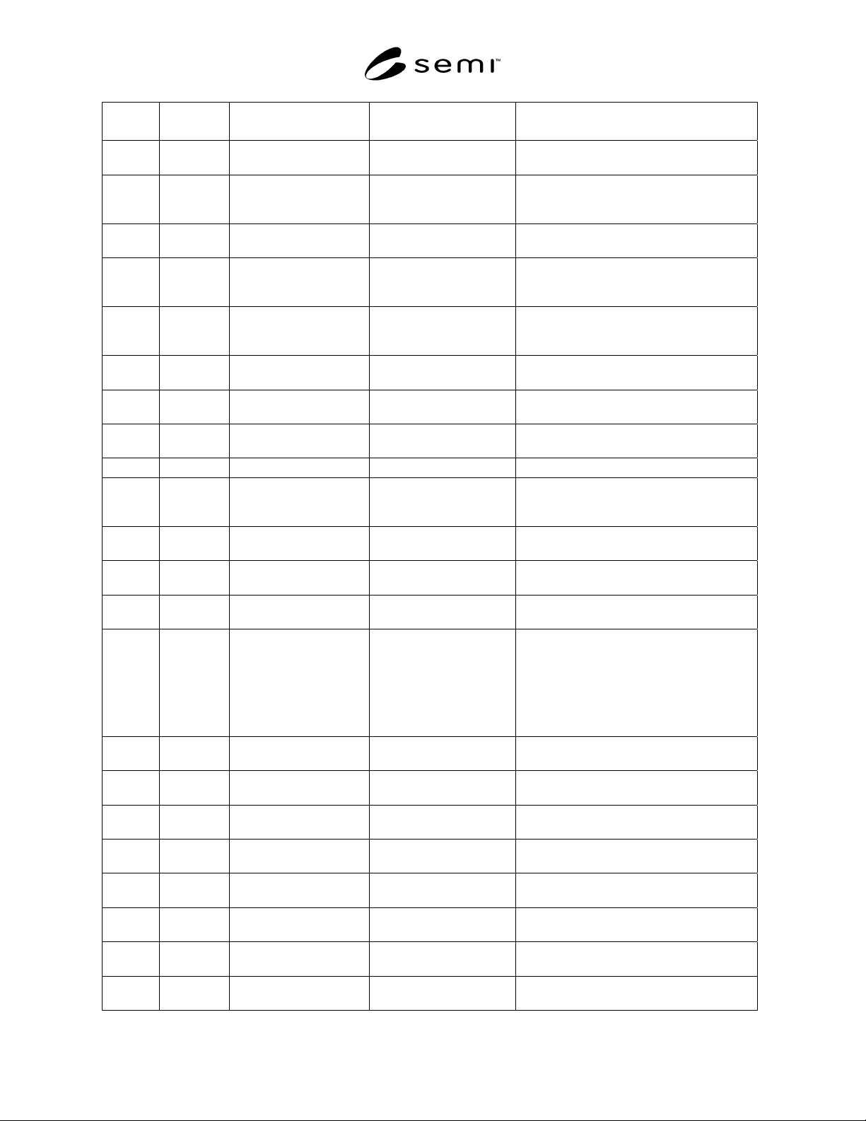
Symbol
Used
Figure
Number
Value Specified Datum Measured from Boundary or Feature Measured to
x3† 1, 10, 12 125 mm (4.92 in.)
minimum
bilateral datum plane inside of front cassette side domains
x4‡ 1, 10, 12 8 mm (0.31 in.)
minimum
farthest protrusion of
cassette from bilateral
datum plane
encroachment of cassette side domain on
side grip pits
x5 2, 4 76 ± 1 mm
(2.99 ± 0.04 in.)
bilateral datum plane outside of cassette top and bottom domains
above and below rear cassette side domains
x6 2, 4, 9 112.5 mm (4.43 in.)
maximum
bilateral datum plane encroachment of cassette top and bottom
domains on near side of vertical optical
wafer sensing paths
x7‡ 2, 10 12 mm (0.47 in.)
minimum
farthest protrusion of
cassette from bilateral
datum plane
encroachment of cassette top domain on
space underneath robotic handling flanges
x8* 5 12.5 mm (0.49 in.) bilateral datum plane end of line segment along center of center
cassette sensing pad
x9 1, 2, 4, 10,
12
167 mm (6.57 in.)
maximum
bilateral datum plane left and right side of cassette
x10‡ 1, 10, 12 166 ± 1 mm
(6.54 ± 0.04 in.)
bilateral datum plane rim of opening of side grip pits
x11 4, 12 166 mm (6.54 in.) bilateral datum plane origin of radius of fork-lift pin hole
x12 4, 9 125 mm (4.92 in.)
minimum
bilateral datum plane encroachment of cassette bottom domain on
far side of vertical optical wafer sensing
paths
x13* 5 88.5 mm (3.48 in.) bilateral datum plane near end of line segment along center of
front cassette sensing pads
x14* 5 118.5 mm (4.67 in.) bilateral datum plane far end of line segment along center of front
cassette sensing pads
x15 4, 12 132 mm (5.2 in.)
maximum
bilateral datum plane intersection of cassette bottom domain and
conveyor rail
x16 4, 12 140 ± 1 mm
(5.51 ± 0.04 in.)
(required)
140 ± 0.25 mm
(5.512 ± 0.010 in.)
(recommended for
roller conveyors)
bilateral datum plane end of conveyor rail and encroachment of
cassette bottom domain on fork-lift area
x17* 5 17.5 mm (0.69 in.) bilateral datum plane line segment along center of rear cassette
sensing pads
x21* 5 30 mm (1.18 in.) bilateral datum plane origin of radius r14 at center of info pads A
and B
x22* 5 70 mm (2.76 in.) bilateral datum plane origin of radius r17 at center of info pads C
and D
x25‡ 14, 16 30 mm (1.18 in.)
minimum
bilateral datum plane far end of top and bottom cassette
identification tag areas
x27 None ± 1 mm (± 0.04 in.)
flatness over tag area
bilateral datum plane surface of side cassette identification tag
area
y1† 1 3 mm (0.12 in.)
maximum
facial datum plane origin of r2 and r3 on bilateral datum plane
y2‡ 1, 7, 8 10 ± 1 mm
(0.39 ± 0.04 in.)
facial datum plane front wall of side grip pits
y3‡ 1, 7, 8 10 ± 1 mm
(0.39 ± 0.04 in.)
facial datum plane rear wall of side grip pits