semi合集-English.pdf - 第5814页
SEMI P24-94 © SEMI 1994, 2004 5 RELATED INFORMATION 1 NOTICE : The material contained in this related information is not an official p art of SEMI P24 and is not meant to modify or s u persede the st andard in any way. T…

SEMI P24-94 © SEMI 1994, 2004 4
8 Related Documents
“ASTM Compilation of ASTM Standard Definitions,”
American Society for Testing and Materials, 100 Barr
Harbor Drive, West Conshohoken, PA 19428.
Nyyssonen, Dr. Robert D. Larrabee, “Submicrometer
Linewidth Metrology for the Optical Microscope,” (J.
of Research of National Bureau of Standards, Vol. 92,
No. 3, May/June 1987). National Institute of Standards
and Technology (NIST), Bldg. 202, Room 204,
Gaithersburg, MD 20899.
Dr. Robert D. Larrabee and Dr. Michael T. Postek,
“Precision, Accuracy, Uncertainty and Traceability and
Their Application to Submicrometer Dimensional
Metrology” (Solid-State Electronics, Vol. 36, No 5, pp
673-684, 1993).
SEMASPEC #91090709A-ENG, “Introduction to
Measurement Capabilities Studies,” SEMATECH,
Technology Transfer, 2706 Montopolis Drive, Austin,
TX 78741.
SEMI P24-94 © SEMI 1994, 2004 5
RELATED INFORMATION 1
NOTICE: The material contained in this related information is not an official part of SEMI P24 and is not meant to
modify or supersede the standard in any way. This information is provided as a source of information to aid in the
application of the standard. As such, it is to be considered as reference material only. The standard should be
referred to in all cases. This related information was approved for publication by full balloted procedures.
R1-1 Short Term Test Duration
R1-1.1 It is recommended the short term test duration
be 30 measurements done in the shortest possible time
under the most limited of conditions to eliminate
extraneous sources of variation.
R1-2 Long Term Duration
R1-2.1 Common practice requires about 30 degrees of
freedom in the highest level of sources of variation.
For example, one should continue a long term study
over 30 working days, if days is the highest level of
variation.
R1-3 Confidence Interval
R1-3.1 This is one way in which confidence interval is
calculated.
vs
2
x
v
.1
/2
2
2
vs
2
x
v
.
/2
2
where
v = df in the extimated standard deviation,
/2 – the alpha risk accepted for the estimate (1-) is
the “confidence level”, and
X
2
refers to the “chi-square” distribution which fits
variances. The equation is arranged such that the area
under the chi-square distribution is to the right of the
designated value.
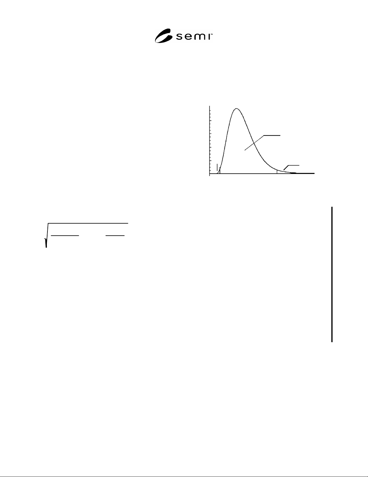
R1-3.2 The reference distribution looks something like
Figure R1-1 — its shape depends on the degrees of
freedom in the estimate.
0
1-
/2
/2
Figure R1-1
Example of a Chi-Square Distribution
NOTICE: SEMI makes no warranties or
representations as to the suitability of the standards set
forth herein for any particular application. The
determination of the suitability of the standard is solely
the responsibility of the user. Users are cautioned to
refer to manufacturer's instructions, product labels,
product data sheets, and other relevant literature,
respecting any materials or equipment mentioned
herein. These standards are subject to change without
notice.
By publication of this standard, Semiconductor
Equipment and Materials International (SEMI) takes no
position respecting the validity of any patent rights or
copyrights asserted in connection with any items
mentioned in this standard. Users of this standard are
expressly advised that determination of any such patent
rights or copyrights, and the risk of infringement of
such rights are entirely their own responsibility.
Copyright by SEMI® (Semiconductor Equipment and Materials
International), 3081 Zanker Road, San Jose, CA 95134. Reproduction of
the contents in whole or in part is forbidden without express written
consent of SEMI.
SEMI P25-94 © SEMI 1994, 2004 1
SEMI P25-94 (Reapproved 1104)
SPECIFICATION FOR MEASURING DEPTH OF FOCUS AND BEST
FOCUS
This specification was technically approved by the Global Micropatterning Committee and is the direct
responsibility of the North American Microlithography Committee. Current edition approved by the North
American Regional Standards Committee on August 16, 2004. Initially available at www.semi.org
September 2004; to be published November 2004. Originally published in 1994.
1 Purpose
1.1 This document provides a common descriptive
vocabulary and outline of basic technique for use by
photolithographers in the IC industry to gauge and
report the depth of focus, astigmatism, and field
curvature of IC photolithographic instruments (e.g.,
scanners, steppers). [Hereafter referred to as
“instrument” or “instruments.”]
2 Scope
2.1 This specification is limited to the measurement of
focus and depth of focus for photolithography as used
in the manufacture of integrated circuits and closely
allied technologies. Because of the wide variation in
equipment techniques, it is not possible to provide a
definitive measurement procedure for these parameters.
Rather, in this document, a basic guideline is offered.
NOTE 1: This technique has value in determining the best
focus setting for a given application, however the main
concern will be the determination for the depth of focus,
astigmatism and field curvature for the purpose of comparing
different instruments and processes.
NOTICE: This standard does not purport to address
safety issues, if any, associated with its use. It is the
responsibility of the users of this standard to establish
appropriate safety and health practices and determine
the applicability of regulatory or other limitations prior
to use.
3 Limitations
3.1 It must be emphasized that the values of depth of
focus, astigmatism, and field curvature cannot be
determined for a given instrument independent of the
effects of the image geometries and the image transfer
process. The values will have to be determined under
the constraints of a practical application process,
suitable for the instrument, illumination, process, object
pattern, and environment. Thus, the process to be used
for a fair measure of instrument performance must be
one that is appropriate and has been optimized for the
given instrument and application. Comparison of the
performance of two different instruments will
inherently be a comparison of the the total application,
instrument specific processes included. A description of
the process is a necessary part of the report of a depth
of focus, astigmatism or field curvature measurement.
Relying on values that were obtained under
significantly different application conditions from the
desired application will result in error and potential
unexpected process failure.
4 Referenced Standards
4.1 SEMI Standards
SEMI P19 — Metrology Pattern Cells for Integrated
Circuit Manufacture
NOTICE: Unless otherwise indicated, all documents
cited shall be the latest published versions.
5 Terminology
5.1 Definitions
NOTE 2: The scope of the following definitions does not
necessarily cover application outside of the procedures
discussed herein. For more universal definitions and
discussion, the user is referred to any of the standard optical
texts.
5.1.1 image (micropatterning) — any single geometric
form appearing in a layout: (1) drafting — as a part of a
master drawing or layout; (2) optical — as projected on
a screen or viewed, usually at some magnification or
reduction; (3) oxide — as etched in the silicon dioxide
layer on an oxidized silicon wafer; (4) photographic —
as in a photomask or in the emulsion of a photographic
film or plate; (5) as a photoresist, an exposed and
developed coating on a substrate.
5.1.2 processed image (micropatterning) — any single
geometric form appearing in the realized pattern or
topographical variation in a material surface or material
constitution, obtained by a physical process of pattern
transference from an optical image.
NOTE 3: This definition is intended to extend the discussion
of depth of focus and focus to include both cases where the
images are realized in photoresist films, per the image
definition given above, and cases where there may not in fact
be a photoresist film involved in the optical pattern
transference process. Examples include photoactive chemical
vapor deposition and photo ablation.