semi合集-English.pdf - 第7523页
SEMI MF1727-0304 © SEMI 2003, 2004 4 NOTICE: SEMI makes no warranties or representations as to the suitability o f the standards set forth herei n for any pa rticular application. The determination of the suitability o f…
SEMI MF1727-0304 © SEMI 2003, 2004 3
9 Sampling
9.1 Select specimens to represent the lot to be tested as
specified in producer/consumer agreements.
10 Specimen Preparation
10.1 Commonly this practice may be used for wafers
as they are received; however, the parties using this
practice may establish a uniform cleaning procedure
before oxidation.
11 Preparation of Apparatus
11.1 The oxidation furnace tube (working chamber)
and associated quartzware shall be maintained in a state
suitable for producing oxides appropriate for the
process for which the wafers are being tested.
11.2 Immediately before use, clean the pickup tool
using standard industry practices.
12 Procedure
12.1 Handle wafers only with a clean, nonmetallic
pickup tool or automated transfer unit to avoid
scratching or contaminating the surface.
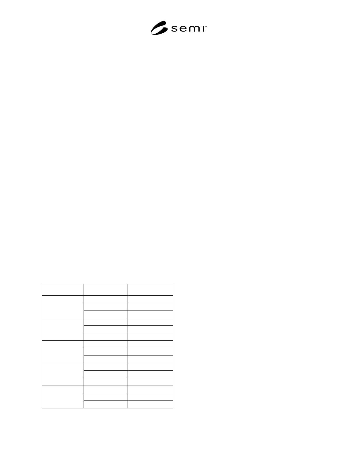
12.2 Oxidize the wafers by the thermal sequence listed
in Table 1 or by a process acceptable to both producer
and consumer.
12.2.1 Caution — Pyrogenic steam oxidation uses
heated hydrogen and oxygen to grow a wet oxide layer.
Improper or uncontrolled combination of these gases
can result in fire or explosion.
12.2.2 Preheat the furnace to the push temperature.
Table 1 Oxidation Procedure
Step Function Conditions
Ambient Dry Oxygen
Temperature 800° C
1. Push (Load)
Push Rate 200 mm/minute
Ambient Dry Oxygen
Ramp Rate + 5° C/minute
2. Temperature
Ramp
Final Temperature 1100° C
Ambient Steam (wet oxide)
Temperature 1100° C
3. Oxidation
Time 60 minute
Ambient Dry Oxygen
Ramp Rate –3° C/minute
4. Temperature
Ramp
Final Temperature 800° C
Ambient Dry Oxygen
Temperature 800° C
5. Pull (Unload)
Pull Rate 200 mm/minute
12.2.3 Load the specimen wafers into the wafer boat,
being careful to avoid binding, scratching, or
contamination.
12.2.4 Insert the boat into the hot zone at the rate called
for in the thermal sequence being employed. The wafer
boat shall be centered in the uniform hot zone.
12.2.5 Follow the ramp up, oxidation, ramp down, and
pull procedures as specified in the thermal sequence
being employed.
12.2.6 Because silicon wafers and quartz accessories
are extremely hot when they are removed from the
oxidation furnace, allow the materials adequate time to
cool before handling.
12.3 Transfer the room temperature wafers from the
quartz boat to a wafer carrier using the pickup tool or
automated transfer unit.
12.4 Remove the thermal oxide layer using
hydrofluoric acid for 2 min followed by water rinse and
spin dry.
12.4.1 Caution — Hydrofluoric acid solutions are
particularly hazardous and specific preventive measures
must be strictly observed. Safety or protective gear
should be worn while handling acid solutions. Safety
requirements vary, but the essential items are: plastic
gloves, safety glasses, face shield, acid gown, and shoe
covers.
12.5 Select and use an appropriate etching solution as
described in SEMI MF1809 to allow defect delineation
while removing 4 µm (or another amount as agreed
upon between the parties to the test) of silicon from the
surface being evaluated.
12.6 Count and report the density of observed defects
using SEMI MF1810.
13 Keywords
13.1 defects; dislocation; epitaxy; hillock;
imperfections; oxidation; preferential etch; shallow pit;
silicon; slip; stacking fault; swirl

SEMI MF1727-0304 © SEMI 2003, 2004 4
NOTICE: SEMI makes no warranties or
representations as to the suitability of the standards set
forth herein for any particular application. The
determination of the suitability of the standard is solely
the responsibility of the user. Users are cautioned to
refer to manufacturer' s instructions, product labels,
product data sheets, and other relevant literature,
respecting any materials or equipment mentioned
herein. These standards are subject to change without
notice.
By publication of this standard, Semiconductor
Equipment and Materials International (SEMI) takes no
position respecting the validity of any patent rights or
copyrights asserted in connection with any items
mentioned in this standard. Users of this standard are
expressly advised that determination of any such patent
rights or copyrights, and the risk of infringement of
such rights are entirely their own responsibility.
Copyright by SEMI® (Semiconductor Equipment and Materials
International), 3081 Zanker Road, San Jose, CA 95134. Reproduction o
f
the contents in whole or in part is forbidden without express written
consent of SEMI.

SEMI MF1771-0304 © SEMI 2003, 2004 1
SEMI MF1771-0304
TEST METHOD FOR EVALUATING GATE OXIDE INTEGRITY BY
VOLTAGE RAMP TECHNIQUE
This test method was technically approved by the Global Silicon Wafer Committee and is the direct
responsibility of the North American Silicon Wafer Committee. Current edition approved for publication by
the North American Regional Standards Committee on December 4, 2003. Initially available at
www.semi.org February 2004; to be published March 2004. Originally published by ASTM International as
ASTM F 1771-97. Last previous edition SEMI MF1392-97 (Reapproved 2002).
1 Purpose
1.1 The technique outlined in this test method is meant
to standardize the procedure, analysis and reporting of
oxide integrity data via the voltage ramp technique
among interested parties. However, since the values
obtained cannot be entirely divorced from the process
of fabricating the test structure, suitable correlations
should be performed based on process needs and
structure selection. This correlation should include
sample size as well as device geometry.
1.2 Measurement of the electrical integrity of oxides
grown on silicon wafers may also be used in-house as a
means of monitoring the quality of furnaces and other
processing steps as well as judging the impact of
changing some processing steps.
1.3 Selection of various edge and area intensive
structures is crucial for isolating the nature of the
defects. Techniques for using such structures to isolate
the nature of detected defects is beyond the scope of
this test method.
1.4 The actual results are somewhat dependent on the
choice of gate electrode. Polysilicon gates have the
advantage of being identical to finished product in
many instances. Even for polysilicon gates, exact
results depend upon values chosen for polysilicon
thickness, doping, and sheet resistance.
2 Scope
2.1 The techniques outlined in this standard are for the
purpose of standardizing the procedure of measure-
ment, analysis, and reporting of oxide integrity data
between interested parties.
2.1.1 This test method makes no representation
regarding actual device failure rates or
acceptance/rejection criteria.
2.1.2 While some suggestions for data analysis are
included in later sections of this test method,
interpretation of results is beyond the scope of this
standard. Any such interpretations should be agreed
upon between interested parties prior to testing. For
example, a variety of failure criteria are included to
permit separation of so-called intrinsic and extrinsic
oxide failures.
NOTE 1: In this regard this test method differs from that
given in SEMI M51, which is focused on application of gate
oxide integrity measurements, as described in this test
method, to determine the density of crystal originated pits in
the wafer under test. SEMI M51 also provides a standardized
procedure for fabricating the MOS capacitors.
2.2 The background of this test method is provided in
Related Information 1.
2.3 This test method covers the procedure for gaging
the electrical strength of silicon dioxide thin films with
thicknesses ranging from approximately 3 nm to 50 nm.
In the analysis of films of 4 nm or less, the impact of
direct tunneling on the current-voltage characteristics,
and hence the specified failure criteria defined in
Section 5.4, must be taken into account. Since oxide
integrity strongly depends on wafer defects,
contamination, cleanliness, as well as processing, the
users of this test method are expected to include wafer
manufacturers and device manufacturers.
2.4 This test method is not structure specific, but notes
regarding options for different structures may be found
in the appendix. The three most likely structures are
simple planar metal-oxide semiconductor (MOS-
capacitors) (fabricated or mercury probe), various
isolation structures (for example, local oxidation of
silicon (LOCOS)), and field effect transistors. This test
method assumes that a low resistance ohmic contact is
made to the backside of each wafer in each case. For a
more detailed discussion of the design and evaluation of
test structures for this test method, the reader is referred
to the EIA/JEDEC Standard 35-1.
2.5 Failure criteria specified in this test method include
both the fixed current limit (soft) and destructive (hard)
types. In the past, use of a fixed current limit of 1 µA or
more virtually ensured measurement of hard failure, as
the thicker, more heavily contaminated oxides of those
days typically failed catastrophically as soon as
measurable currents were passed. The cleaner
processing of thinner oxides now means that oxides will
sustain relatively large currents with little or no
evidence of failure. While use of fixed current limit
testing may still be of value for assessing uniformity