semi合集-English.pdf - 第7419页
SEMI MF1528-1104 © SEMI 2004 5 rights or copyr ights, and the risk of infrin gement of such rights are entirely their own responsibility. Copyright by SEM I® (Semiconductor Equ ipment and Materials International), 3081 Z…
SEMI MF1528-1104 © SEMI 2004 4
two instruments for a period of approximately 5 years.
2
The polished etched samples were cut from a number of
adjacent wafers cut from one crystal. Measurement
conditions were the same as stated in this test method.
The instruments were CAMECA IMS-3f and
CAMECA IMS-4f. One standard deviation was 2.4
10
13
atoms/cm
3
with an average value of 2.0 10
14
atoms/cm
3
resulting in a relative one-standard deviation
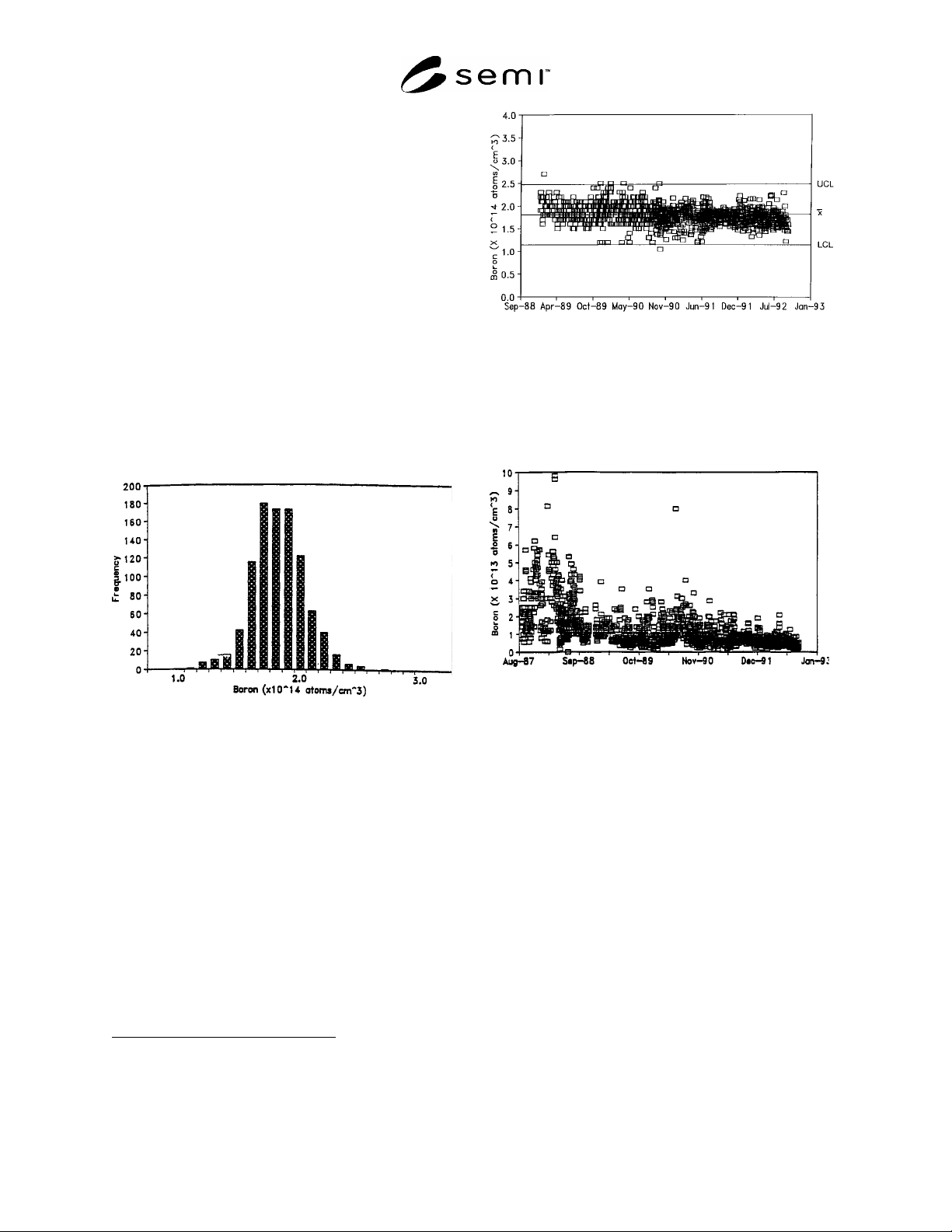
of 12%. The distribution of measurements is shown in
Figure 1. The time sequences of sample and
background measurements are shown in Figure 2 and
Figure 3, respectively.
14.2 Bias — The bias of this measurement cannot be
estimated because there are no absolute standards for
this measurement.
15 Keywords
15.1 boron; epitaxial substrate; silicon; SIMS
Figure 1
Frequency Distribution of Boron Concentration
Over 5-Year Period (Nov 1987 through Sept 1992)
for 900 Samples Cut From Several Adjacent Silicon
Wafers From One Ingot
2 Chu, P. K., Bleiler, R. J., Metz, J. M., Hitzman, C. J., Hockett,
R. S., “Measurement of Boron Contamination in n
+
Silicon
Substrates by Secondary Ion Mass Spectrometry, Abstract 872,”
Extended Abstracts, Vol 93–1, (The Electrochemical Society,
Pennington, NJ, 1993)p. 1285.
NOTE: X-bar is the average of the measurements; UCL is the
upper control limit and equal to the average plus 3 times the
standard deviation; LCL is the lower control limit and equal
to the average minus 3 times the standard deviation.
Figure 2
Boron Concentration Measurement Versus Time
For the Same Sample Set as in Figure 1
Figure 3
Boron Background Concentration as Measured in a
BLANK Sample ([B] < 5
10
12
atoms/cm
3
) Versus
Time Over 5-Year Period (Nov 1987 Through Sept
1992)
NOTICE: SEMI makes no warranties or
representations as to the suitability of the standards set
forth herein for any particular application. The
determination of the suitability of the standard is solely
the responsibility of the user. Users are cautioned to
refer to manufacturer's instructions, product labels,
product data sheets, and other relevant literature,
respecting any materials or equipment mentioned
herein. These standards are subject to change without
notice.
By publication of this standard, Semiconductor
Equipment and Materials International (SEMI) takes no
position respecting the validity of any patent rights or
copyrights asserted in connection with any items
mentioned in this standard. Users of this standard are
expressly advised that determination of any such patent

SEMI MF1528-1104 © SEMI 2004 5
rights or copyrights, and the risk of infringement of
such rights are entirely their own responsibility.
Copyright by SEMI® (Semiconductor Equipment and Materials
International), 3081 Zanker Road, San Jose, CA 95134. Reproduction
of the contents in whole or in part is forbidden without express
written consent of SEMI.

SEMI MF1529-1104 © SEMI 2004 1
SEMI MF1529-1104
TEST METHOD FOR SHEET RESISTANCE UNIFORMITY EVALUATION
BY IN-LINE FOUR-POINT PROBE WITH THE DUAL-CONFIGURATION
PROCEDURE
This test method was technically approved by the Global Silicon Wafer Committee and is the direct
responsibility of the North American Silicon Wafer Committee. Current edition approved for publication by
the North American Regional Standards Committee on August 16, 2004. Initially available at
www.semi.org
September 2004; to be published November 2004. Original edition published by ASTM International as
ASTM F 1529-94. Last previous edition SEMI MF1529-02.
1 Purpose
1.1 The sheet resistance of epitaxial, implanted,
diffused or deposited films is an important materials
acceptance and process control parameter. The
uniformity across a wafer of the sheet resistance
resulting from any of these processes is important for
the equivalence of performance of devices or circuits
made from various regions of the wafer.
1.2 This test method uses a four-point probe in a
manner different from that of other ASTM methods for
the measurement of the resistivity or sheet resistance of
semiconductors. In this test method, two different ways
(configurations) of connecting the probe pins to the
electronics that supply current and measure voltage are
used at each measurement location on the specimen.
This use of a four-point probe is often referred to as
“dual-configuration” or as “configuration switched”
measurements.
1.3 There are three benefits that result from the second
measurement configuration at each location: (1) the
probe no longer needs to be in a high symmetry
orientation on the specimen, that is, being perpendicular
or parallel to the radius on a circular wafer or to the
length or width of a rectangular specimen, as long as it
is a modest distance from the edge of the wafer, (2) the
lateral dimension(s) of the specimen, and the exact
location of the probe on the specimen no longer have to
be known—the geometric scaling factor results directly
from the two sets of electrical measurements at each
location, (3) the two sets of measurements self-correct
for the actual separations between the probe pins in a
manner that has been shown to be more effective than
measuring probe impressions made on a piece of
polished material. As a result, high precision
measurements can be made with smaller probe
separations than is possible with single configuration
use of a four-point probe, thus allowing higher spatial
resolution of wafer sheet resistance variations.
1 Perloff, D. S., “Four-Probe Correction Factors for Use in
Measuring Large Diameter Doped Semiconductor Wafers,” J.
Electrochem. Soc. 123, 1745–1750 (1976).
1.4 This test method is intended primarily for assessing
the uniformity of layers formed by diffusion, epitaxy,
ion implant and chemical vapor, or other deposition
processes on a silicon substrate. The deposited film,
which may be single crystal, polycrystalline or
amorphous silicon, or a metal film, must be electrically
isolated from the substrate. This can be accomplished
if the layer is of opposite conductivity type from the
substrate or is deposited over a dielectric layer such as
silicon dioxide. This test method is capable of
measuring films as thin as 0.05 m, but particular care
is required for establishing reliable measurements for
most films in the range below 0.2 m. Films that have
a thickness up to half the probe separation can be
measured without the use of a thickness-related
correction factor. It may give misleading results for
films formed by silicon on insulator technologies
because of charge or charge trapping in the insulator.
1.5 This test method can be used to measure the sheet
resistance uniformity of bulk substrates. However, the
thickness of the substrate must be known to be constant
or must be measured at all positions where sheet
resistance values are measured in order to calculate
relative variations in resistance reliably.
NOTE 1: The thickness correction factor for layers that are
thicker than 0.5 times the probe spacing is known to vary
more rapidly than that for single-configuration four-probe
measurements, but such a correction has not yet been
published. Until such a correction is published, resistivity
values determined by the dual-configuration method will not
be accurate for these thicker specimens; however, if the wafer
has uniform thickness, variations of resistivity can still be
determined by this test method.
1.6 This test method is suitable for use in materials
acceptance, equipment qualification, process control,
research, and development.
2 Scope
2.1 This test method covers the direct measurement of
the sheet resistance and its variation for all but the
periphery (amounting to three probe separations) for
circular conducting layers pertinent to silicon
semiconductor technology. These layers may be