semi合集-English.pdf - 第5752页
SEMI P19-92 © SEMI 19 92, 1996 3 3.1.6 Labels, border l ines, i ndicator m a r ks, or any other adjacent f eature will be separated by a minimum of 5 µm . 3.1.7 A label to indicate the nomina l fe ature width must be pla…

SEMI P19-92 © SEMI 1992, 1996 2
isolated line — a clearfield, dark line as shown in
Figure 2 (SYN: island).
Figure 2
Isolated Line
isolated space — A darkfield, clear line as shown in
Figure 3 (SYN: window, trench, contact, opening).
Figure 3
Isolated Space
2 Detail Specification
2.1 Introduction
2.1.1 This specification describes th e pattern cells,
which are illustrated in the figures at the end of this
document. These cells are to be placed
photolithographically or by other direct patterning
methods onto wafer substrates at different masking
levels during the IC manufacturing process.
2.1.2 Many details of the pattern cel ls, such as the
orientation, magnitude, range of the linewidths, and
polarity of tone (clearfield vs. darkfield) will be defined
by the user, unless otherwise noted. When reporting
results based on tests using these cells, details such as
field polarity, orientation, and topographic
considerations must be indicated.
2.1.3 All critical dimensions given i n this document
are the actual CAD values at 1X. For a given
magnification, M, the target dimensions on the reticle
should be exactly M times the dimension given in this
specification. The reticle dimensions must not be sized
to compensate for any wafer process-induced bias.
2.2 Applications
2.2.1 These cells are intended to be used in several
applications. The following applications list some of the
intended uses for the pattern cells.
2.2.1.1 in-line process monitoring — To establish
patterns to determine if the layer has been processed to
design specifications.
2.2.1.2 process transfer — To standardize the patterns
for process monitoring within manufacturing
fabrication sites and to facilitate process and technology
transfers between sites.
2.2.1.3 equipment evaluation — To standardize the
patterns used to evaluate semiconductor equipment.
2.2.1.4 equipment characterization — To standardize
the patterns for the characterization process of different
metrology equipment.
3 Guidelines for Application s
3.1 General
3.1.1 The cells described here repres ent a primary
metrology set from which composite patterns may be
constructed.
3.1.2 A composite pattern set meets this standard if it
consists of any number of the basic cells described
herein, provided all design rules for each cell are
obeyed.
3.1.3 Each basic cell contains a fundamental design
feature. This feature may be repeated at different (user-
defined) dimensions within a modified metrology cell.
The user will determine all appropriate dimensions for
the feature as they apply to specific
processing/equipment situations.
3.1.4 The figures provided within th is document are
intended to illustrate the proper layout of each pattern
cell and to define the appropriate design elements used
within each basic cell. The pattern cell dimensions are
provided when appropriate.
3.1.5 All feature groups must be separated by at least
five times the largest feature width. This proximity rule
is defined in order to ensure that patterns intended to be
independent are indeed non-coupled.
SEMI P19-92 © SEMI 1992, 19963
3.1.6 Labels, border lines, indicator marks, or any
other adjacent feature will be separated by a minimum
of 5 µm.
3.1.7 A label to indicate the nomina l feature width
must be placed near each basic cell, except the linearity
cell, which has no user-defined features. The units of
the CD labels must be micrometers and at least two
significant figures must be used. The labels must be of
a clearly printable size. Decimal points are optional. If
decimal points are eliminated, digits to the left of the
imaginary decimal point must be slightly larger than
those digits to the right. Characters to the left of the
decimal are optional. All CD labels that are printed with
one size only will correspond to numbers less than 1.0
µm, and any number greater than 1.0 µm must contain
at least one character to the right of the decimal place.
If the cell includes a bias, a label to indicate this bias,
including a “+” sign, must be placed near the basic cell.
One significant figure may be used for bias labels if the
bias is less than 1.0 µm and a multiple of 0.1 µm. (e.g.,
+ 4 = + 0.4 µm).
3.1.8 It is recognized that there are design limitations
dictated by the equipment used to generate the pattern
(e.g., CAD grids, PG rectangles, E-beam spot sizes). It
is permitted within this standard to modify these cells in
order to meet these equipment limitations (e.g., stay on
grid).
3.2 Specific
3.2.1 L-Bar Cell — (See Figure 4.)
3.2.1.1 The L-bar cell is designed to b e a measurement
site for isolated features as well as line and space
groups in orthogonal axes. The cell can be used to
measure the quality of pattern transfer and metrology of
imaged features. The cell is also a qualitative visual test
site for resolution of straight lines and lines bent at right
angles.
3.2.1.2 The design elements are the no minal feature
width, the inter-feature spacing, the minimum feature
length, and the intergrouping linewidth difference
(bias).
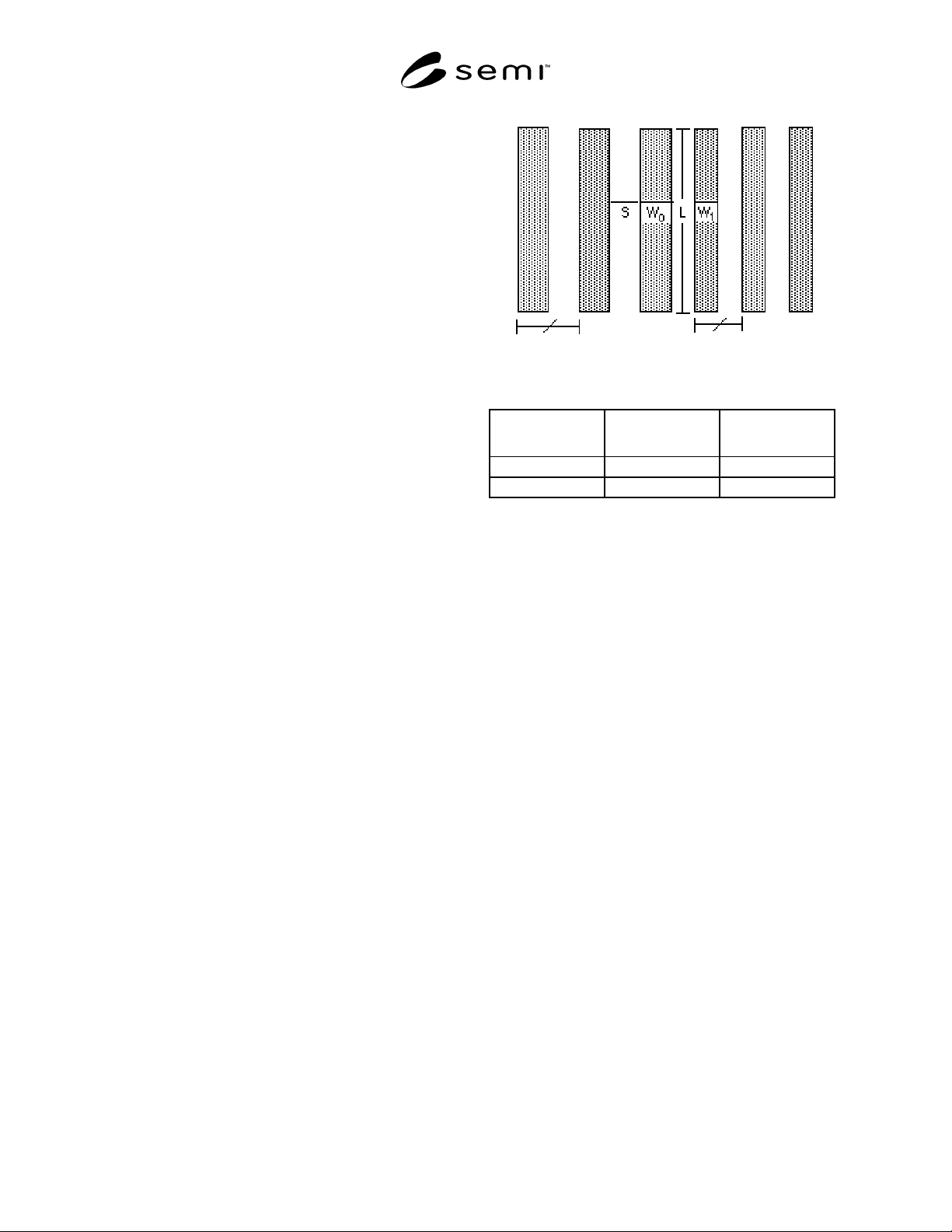
3.2.1.3 The basic cell consists of one o r more groups
of nested L-shaped lines at a specific pitch. The pitch is
defined at twice the nominal feature width. (See Figure
5.)
W
0
= Nominal feature width
S = Interfeature spacing
L = Nominal feature length
W
0
-W
1
= Intergrouping linewidth difference (bias)
Figure 5
Table 1
Nominal Feature
Width
Number of Nested
L-bars Minimum Length
>1 µm 3 10 W
0
≤1 µm 5 10 µm
The center L-bar of each group shall extend beyond the
ends of the other L-bars by at least 10 µm. If these
cells are to be used for cross-section analysis, the length
of the L-bars may be designed considerably longer than
the minimum length.
3.2.1.4 The L-bar basic cell consists o f one, three,
five, or seven feature groups. If the basic cell only
consists of a single feature group, then the lines and
spaces must both be equal to the nominal feature width.
If the basic cell consists of three, five, or seven groups,
then the groups are nested. For the middle group, the
lines and spaces must both be equal to the nominal
feature width. The feature widths in each successive
feature group nested outside the middle group are
incrementally increased by the bias. The feature widths
in each successive feature group inside the middle
group are incrementally decreased by the bias. The
pitch for all L-bar groups within a basic cell must be
held constant and equal to twice the nominal feature
width.
3.2.2 Straight-Line Cell — (See Figure 6.)
3.2.2.1 The straight-line cell is a versi on of the L-bar
cell, modified for tilted SEM inspection by removing
the elbows.
SEMI P19-92 © SEMI 1992, 1996 4
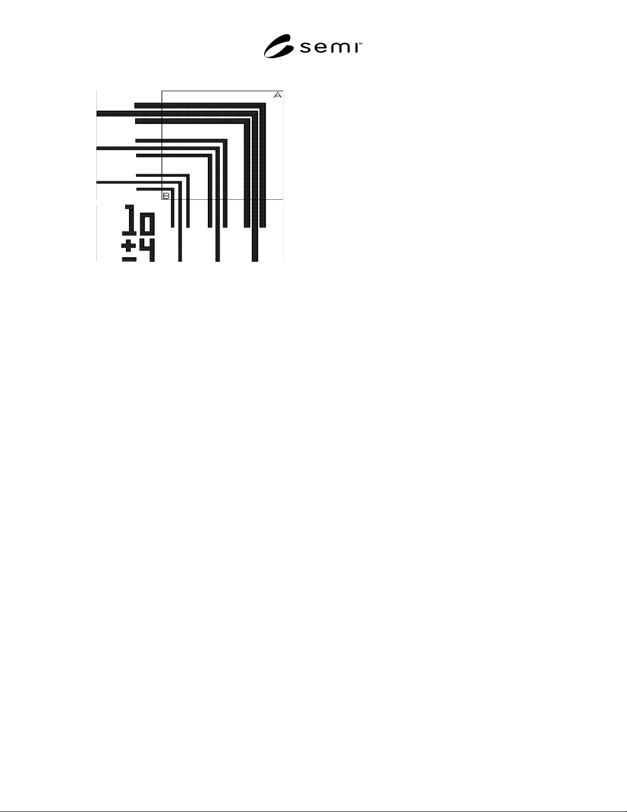
Figure 7
The square area, shown above, is removed to create
straight-line cell.
3.2.2.2 To create the straight-line cell from the L-bar
cell, the area removed will be a square defined by two
diagonal corners referred to as “A” and “B” in Figure 7.
Corner “A” is the outer edge of the outermost elbow.
Corner “B” is a point inside the innermost elbow whose
distance to the nearest edge is five times that of the
smallest CD — or 5.0 µm if the smallest CD is less than
1.0 µm. This square area must remain unpatterned.
3.2.3 Proximity Dagger Cell — (See Figure 8.)
3.2.3.1 The proximity dagger cell is designed to
provide information on the proximity effects of isolated
lines/spaces in relation to large area blocks. This cell
design allows clear and dark features to be measured
simultaneously in one layout.
3.2.3.2 The design elements within the cell are the
nominal feature linewidth, the nominal feature
spacewidth, and the staircase stepwidth. The stepwidth
is user-selected, but it is recommended to be at least
25% of the nominal feature pitch (i.e., pitch equals
nominal linewidth plus nominal spacewidth).
3.2.3.3 The cell consists of a nine-tier staircase
reproduced symmetrically in both clear and darkfields.
A full description of the clearfield staircase (i.e., large
chrome islands) is given. The same descriptions apply
for the darkfield staircase except the polarities are
reversed. Each tier is 10 microns tall. The full width of
the cell is 40 microns and the full height is 180 microns.
The first tier separates the nominal feature width
symmetrically from the large chrome islands by an
amount equal to the nominal width. Tiers 2–7 are
successively wider by the indicated bias. The 8th and
9th tiers will be 5 and 10 times the nominal feature
width respectively.
3.2.4 Contact Array Cell — (See Figure 9.)
3.2.4.1 The contact array cell is desig ned to provide
resolution and proximity-effect information over a wide
range of contact sizes.
3.2.4.2 The design elements are the no minal square
contact dimension, the inter-contact dimension within
the 5 × 5 and the 3 × 3 arrays. The latter dimension
will be equal to the contact dimension.
3.2.4.3 The contact array cell will consist of three
subgroups: a 5 × 5 contact array, a 3 × 3 contact array,
and an isolated contact. The 5 × 5 array will produce
the maximal proximity (i.e., dense printing) for the
center contact. The center contact in the 3 × 3 array
will exhibit proximal printing effects different from
both the isolated contact and the dense contact.
3.2.5 Staggered Contact Array — (See Figure 10.)
3.2.5.1 The staggered contact array ce ll is designed to
improve the probability of cross-sectioning small
contacts for SEM metrology analysis.
3.2.5.2 The design elements are the sq uare contact
dimension, the column-to-column vertical offset — or
staggering — and the contact-to-contact spacing. The
contact-to-contact spacing will be equal to the square
contact dimension.
3.2.5.3 The contacts are laid out using a minimum of
three columns of contacts. The user-selected offset
between columns should allow the contacts to remain
on grid.
3.2.5.4 The lines (or spaces) shown on the left side of
Figure 10 are optional. They have been placed to
provide feature identification of pitch calibration. If the
widths are to be submicron, 5 lines (or spaces) instead
of 3 will be required.
3.2.6 Linearity Cell — (See Figure 1 1.)
3.2.6.1 The linearity cell is designed to test (1) the
linearity of the measurement method, assuming the
lithographical process is linear over all line sizes used,
or (2) the linearity of the process, assuming that the
metrological method is linear over all line sizes used.
3.2.6.2 The design elements of this cell are the
linewidths, the interfeature spacing, and the minimum
line lengths. Unlike the other cells, its elements are not
adjusted to a nominal critical dimension, but rather are
numerically specified as constants for all applications.
3.2.6.3 The cell consists of nine parallel lines, placed
on a five-micron pitch. The linewidths are 1.2, 1.1, 1.0,
0.9, 0.8, 0.7, 0.6, 0.5, and 0.4 microns. The line lengths
are a minimum of ten microns. A two-micron top and
bottom border (running orthogonal to the parallel lines,