semi合集-English.pdf - 第6170页
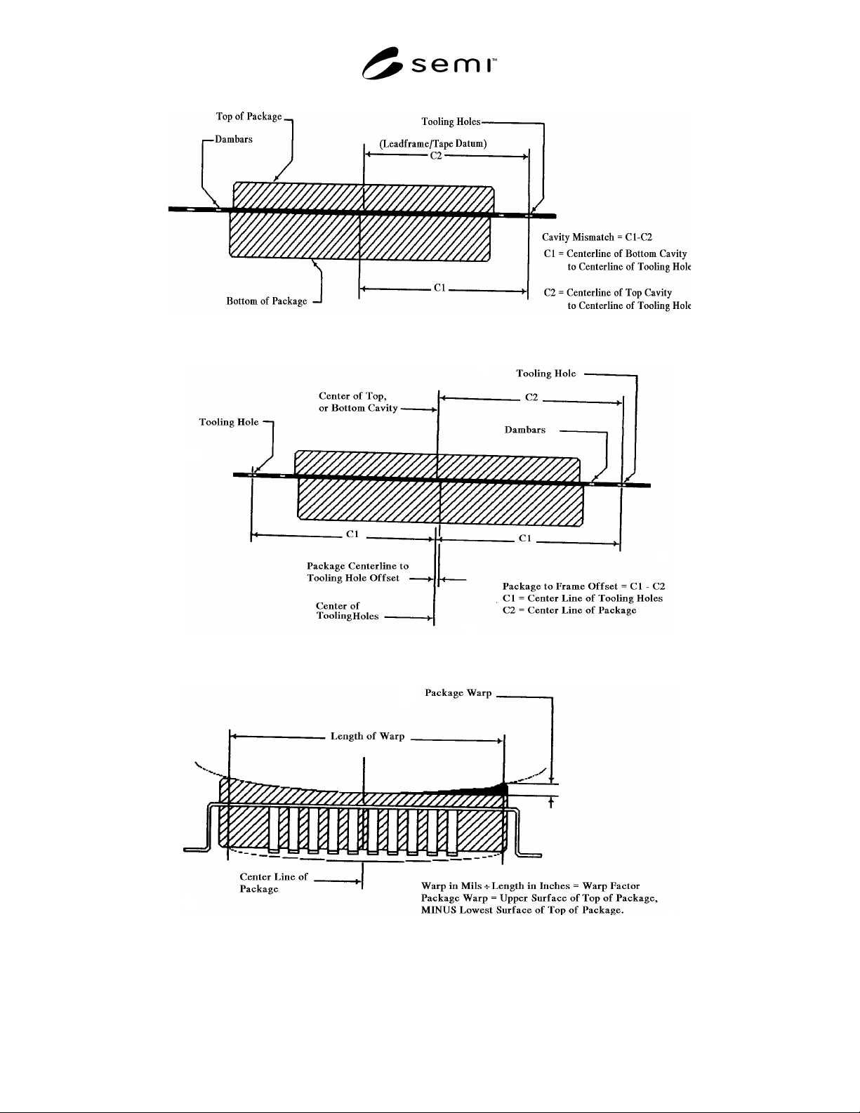
SEMI G36-88 © SEMI 198 6, 1988 3 Figure 1 Top to Bot to m Cavity Mism atch Figure 2 Cavity to Fram e Offset Figure 3 Package Warp age
SEMI G36-88 © SEMI 1986, 1988 2
8. Molding press to be used.
9. Electrical power available for heating.
10. Applicable leadframe drawing, including all
dimensions.
5 Dimensions
5.1 Drawing must show dimensions for the following
items, if applicable:
1. Package length
2. Package width
3. Top cavity thickness
4. Bottom cavity thickness
5. Frame thickness
6. Top ejector pin locations from datum lines
7. Bottom ejector pin locations from datum lines
8. Ejector pin sizes (top and bottom)
9. Ejector depth (top and bottom, draft angle top and
bottom side)
10.Pin 1 ID location from package center
11.Pin 1 ID shape and size
12.All applicable package radii
13.Draft angles (top and bottom)
14. Package parting line location
15.Shoulder bend location
6 Product Criteria
6.1 Dimensional tolerance limits for high density TAB
products (see Section 3).
6.1.1 Recognizing that every manufacturing process is
subject to variation, the following list details the
acceptable limit of this variation:
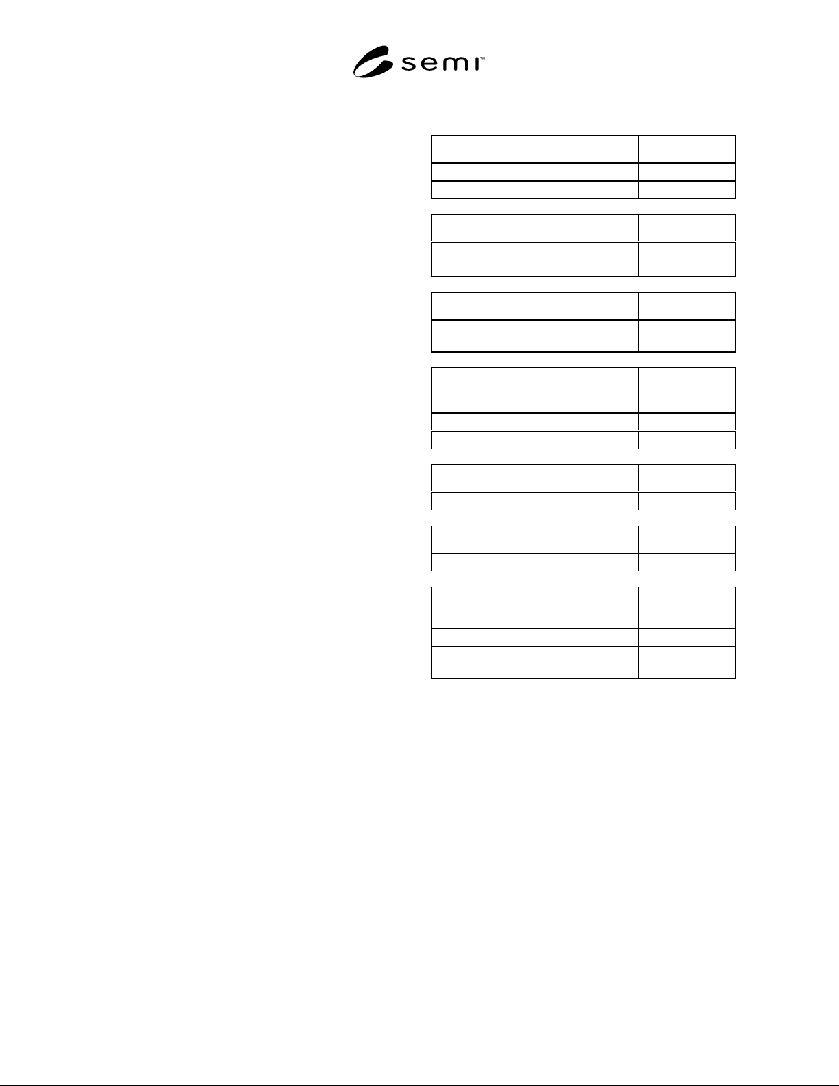
28-328 LEAD
OVERLAP/OFFSET
Cavity Overlap (See Figure 1) 0.002" (maximum)
Cavity Mismatch (See Figure 1 0.002" (maximum)
CAVITY TO FRAME OFFSET
(See Figure 2)
(not including leadframe tolerances)
0.002" (maximum)
PACKAGE WARPAGE
Warp factor (See Figure 3) 2.5 to a max. of
0.003"
PROTRUSIONS & INTRUSIONS
(See Figure 4) Parting line 0.005" (maximum)
Gating 0.005" (maximum)
Top or bottom ejector pin 0.002" (maximum)
VARIATIONS IN LEAD POSITION
(See Figure 4) 0.003" (maximum)
LEAD COPLANARITY
(See Figure 6) 0.002" (maximum)
DAMBAR TRIMMING
INTRUSIONS/PROTRUSIONS
Intrustions (See Figure 6) 0.002" (maximum)
Protrusions (See Figure 4) (shall not
decrease gap more than 20%)
0.003" (maximum)
7 Packaging
Tooling must be packed in containers designed and
constructed to prevent damage and/or contamination.
SEMI G36-88 © SEMI 1986, 19883
Figure 1
Top to Bottom Cavity Mismatch
Figure 2
Cavity to Frame Offset
Figure 3
Package Warpage
SEMI G36-88 © SEMI 1986, 1988 4
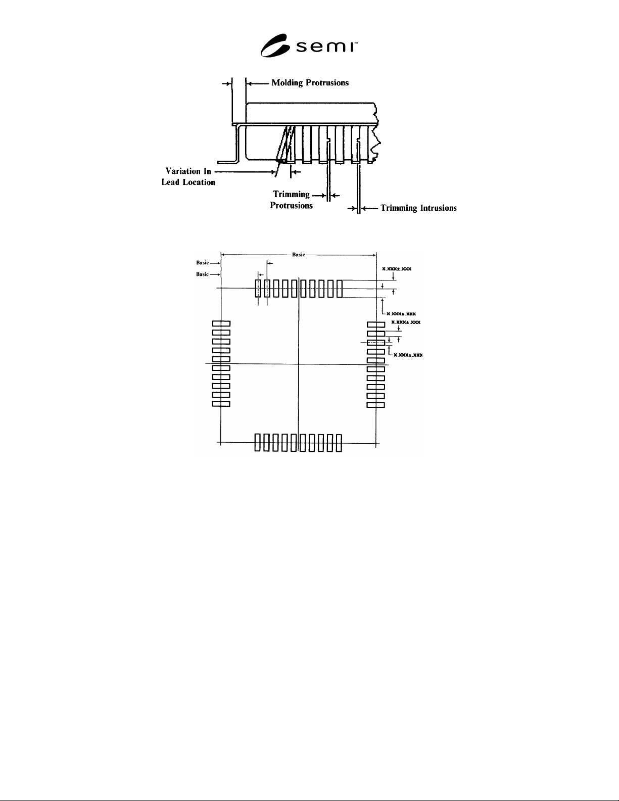
Figure 4
Parting Line Protrusion/Intrusion and Variation in Lead Location
Figure 5
Lead Position Overlay Example
NOTICE: These standards do not purport to address safety issues, if any, associated with their use. It is the
responsibility of the user of these standards to establish appropriate safety and health practices and determine the
applicability of regulatory limitations prior to use. SEMI makes no warranties or representations as to the suitability
of the standards set forth herein for any particular application. The determination of the suitability of the standard is
solely the responsibility of the user. Users are cautioned to refer to manufacturer’s instructions, product labels,
product data sheets, and other relevant literature respecting any materials mentioned herein. These standards are
subject to change without notice.
The user’s attention is called to the possibility that compliance with this standard may require use of copyrighted
material or of an invention covered by patent rights. By publication of this standard, SEMI takes no position
respecting the validity of any patent rights or copyrights asserted in connection with any item mentioned in this
standard. Users of this standard are expressly advised that determination of any such patent rights or copyrights, and
the risk of infringement of such rights, are entirely their own responsibility.
Copyright by SEMI® (Semiconductor Equipment and Materials
International), 3081 Zanker Road, San Jose, CA 95134. Reproduction o
f
the contents in whole or in part is forbidden without express written
consent of SEMI.