semi合集-English.pdf - 第7546页
SEMI MF1809-0704 © SEMI 2003, 2004 11 RELATED INFORMATION 1 RELATIONSHIPS BETWEEN SEMI MF1809 AND JIS H-0609 NOTICE: This related info rmation i s not an official part of SEMI MF1809. It was developed by the task force d…
SEMI MF1809-0704 © SEMI 2003, 2004 10
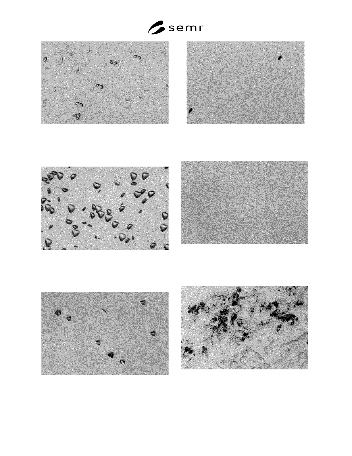
Low Resistivity Boron Doped (100) Wafer; 1100° C Steam,
80 minute Oxidation; Wright Etch with Agitation
Figure 27
Oxidation Stacking Faults, 500
×
(111) Wafer; 1100° C Steam, 80 minute Oxidation; Wright
Etch with Agitation
Figure 28
Oxidation Induced Stacking Faults, 500
×
(111) Wafer; Wright Etch with Agitation
Figure 29
Slip Dislocations, 500
×
(100) Wafer; Wright Etch with Agitation
Figure 30
Slip Dislocations, 200
×
Boron doped (100) Wafer; 1100° C Steam, 80 minute
Oxidation; Wright Etch with Agitation
Figure 31
Shallow Pits (Haze), 500
×
Boron Doped Wafer; Wright Etch
Figure 32
Etching Stain Artifact, 200
×
SEMI MF1809-0704 © SEMI 2003, 2004 11
RELATED INFORMATION 1
RELATIONSHIPS BETWEEN SEMI MF1809 AND JIS H-0609
NOTICE: This related information is not an official part of SEMI MF1809. It was developed by the task
force during the revision of the document in 2003. This related information was approved for publication
by full letter ballot on April 22, 2004.
R1-1 Both this guide and test method JIS H-0609
identify etching solutions for use in delineating
structural defects in silicon. As indicated in 2.3, this
guide is intended to be used with other practices and
test methods while JIS H-0609 covers the entire
delineation and counting process.
R1-2 JIS H-0609 contains sections on terminology,
sample preparation, including thermal oxidation, selec-
tion of etchants, etching procedures, measurement loca-
tions, and measurement methods for various crystalline
defects.
R1-2.1 The definitions of the various crystal defects
are generally similar to those in SEMI MF1241 with
only minor differences in emphasis.
R1-2.2 Sample preparation and etching procedures are
similar in most respects to the procedures in SEMI
MF1725, SEMI MF1726, and (for thermal oxidation)
SEMI MF1727. The minor differences in definitions
are not considered to be technically significant.
R1-2.3 JIS H-0609 covers only non-chromic etching
solutions that differ from those covered in this guide.
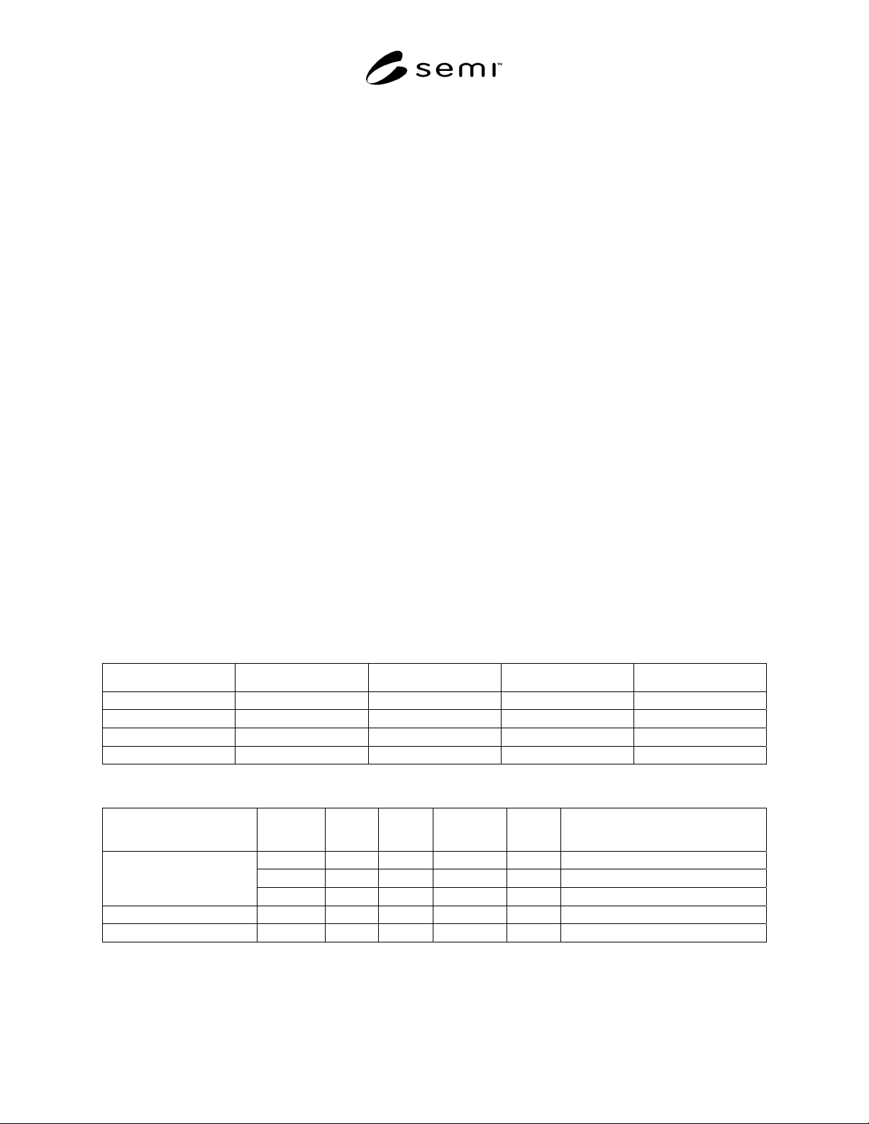
Tables R1-1 and R1-2 list the etching solutions
discussed in JIS H-0609. Detailed discussions of the
suitability of the various etching solutions and
microphotographs of exposed crystal defects are
provided in JIS H-0609, similarly to the manner in
which similar information is provided in this guide.
Although JIS H-0609 does not cover the use of chrome-
containing etching solutions, it does contain com-
parisons with the etch rates of several chrome-con-
taining etching solutions, including Secco, Wright, and
Sirtl etches (see Section 9 for references to these
etching solutions).
R1-2.4 JIS H-0609 covers a variety of different mea-
suring locations and counting procedures for various
different crystal defects, unlike SEMI MF1810, which
describes only a method for counting etch pits in a
specified pattern. Visual inspection of some defect
types is recommended by JIS H-0609; such visual
inspection is also covered in SEMI MF523. JIS H-0609
includes a discussion of observation of denuded zone,
but because of the variety of technologies in place for
this aspect, no standardized measurement method is
defined.
Table R1-1 Composition of preferential etching solutions (I) (volume ratio) from JIS H-0609
Etching Solution Hydrofluoric Acid Nitric Acid Acetic Acid Water
A 1 12.7 3 3.7
B 1 12.7 3 5.7
C 1 12.7 1 6.7
D 2 12.7 2 6.7
Table R1-2 Composition of preferential etching solutions (II) (volume ratio) from JIS H-0609
Applicable Wafer
Dopant, Crystal Surface
Etching
Solution
HF HNO
3
CH
3
COOH H
2
O
Additive Reagent Name:
Concentration
E(Note 1) 1 2.5 — 10.5 AgNO
3
: 0.005 mol/L(Note 2)
F(Note 1) 3 5.1 — 7.9
B (100)
G 1 12.7 — 6.3
Sb (100) H 2 5.9 2 6.1 KI: 0.1~ 0.5 g/L(Note 3)
Sb (111) I 2 6.8 2 6.2 KI: 0.1~ 0.5 g/L(Note 3)
NOTE 1: E and F Etches form a stain film. The stain film can be removed by rinsing the stained wafer and dipping it into B Etch for 5~ 10 s.
NOTE 2: By mixing 8 mL of 0.005 mol/L silver nitrate (AgNO
3
) aqueous etching solution into E Etch, the starting time of the reaction can be
advanced.
NOTE 3: By mixing 0.1~ 0.5 g/L potassium iodide (KI) to H and I Etches, stain film formation can be suppressed.

SEMI MF1809-0704 © SEMI 2003, 2004 12
RELATED INFORMATION 2
GUIDELINES FOR SPONSORS OF ADDITIONAL ETCHING
SOLUTIONS
NOTICE: This related information is not an official part of SEMI MF1809. It was developed during the original
development of the document. This related information was approved for publication by full letter ballot on April
22, 2004.
R2-1 A sponsor of additional etching solutions shall
submit tabular information and pictures of etched defect
examples (see Figures 1–32) to the SEMI staff engineer
or coordinator for the Silicon Wafer Committee as
follows:
R2-1.1 A preferential etching solution submitted as an
addition to this guide must be sponsored by an
individual willing to supply information for Tables 1
and 3 or Tables 2 and 4 as appropriate for the type of
etching solution.
R2-1.2 Defect pictures, approximately 2 by 3 in. (50
mm by 75 mm) in size, demonstrating the applications
of the solution shall include the following descriptive
information:
• Image magnification (approximately 400×
preferred),
• Surface removal during etch (in micrometers),
• Relevant sample history (that is, thermal cycle
type, resistivity, agitation, etc.), and
R2-1.3 Images submitted should include OISF' s and
dislocations for (100) and (111) surfaces and, in
addition as available, shallow pits (s-pits), hillocks,
artifacts, and epitaxial defects.
NOTICE: SEMI makes no warranties or
representations as to the suitability of the standards
set forth herein for any particular application. The
determination of the suitability of the standard is
solely the responsibility of the user. Users are
cautioned to refer to manufacturer' s instructions,
product labels, product data sheets, and other
relevant literature, respecting any materials or
equipment mentioned herein. These standards are
subject to change without notice.
By publication of this standard, Semiconductor
Equipment and Materials International (SEMI)
takes no position respecting the validity of any
patent rights or copyrights asserted in connection
with any items mentioned in this standard. Users
of this standard are expressly advised that
determination of any such patent rights or
copyrights, and the risk of infringement of such
rights are entirely their own responsibility.
Copyright by SEMI® (Semiconductor Equipment and Materials
International), 3081 Zanker Road, San Jose, CA 95134. Reproduction o
f
the contents in whole or in part is forbidden without express written
consent of SEMI.