semi合集-English.pdf - 第5页
SEMI E1-0697 © SEMI 1979, 2003 3 Figure 1 Wafer Carrier Outline — General Usage NOTE: Used in conjunction with Tab le 1. Table 2 Symbols Outline F or Auto Transport Usage Specifications Figure 1A Reference Description Ov…
SEMI E1-0697 © SEMI 1979, 2003 2
2.2.18 pocket depth — The distance from the pocket
flat to its own pocket nose, not to the opposite pocket.
(See Figure 1, C2.)
2.2.19 pocket flat — The width of the pocket along the
vertical walls at its narrowest distance. (See Figure 1,
C3.)
2.2.20 pocket nose — The top of the mass of material
between adjacent pockets.
2.2.21 pocket nose radius — The radius on the pocket
nose.
2.2.22 pocket size — The distance between opposite
pocket flats. (See Figure 1, C4.)
2.2.23 pocket spacing — The distance between pocket
centerlines. (See Figure 1, B2.)
2.2.24 pocket width — The width of the pocket at its
widest distance. (See Figure 1, C1.)
2.2.25 top face — The plane or surface of the carrier
from which side wafers enter into or out of the carrier.
2.2.26 track clearance — The unobstructed area
between the two carrier sides on the bar end. (See
Figure 1, D6; Figure 1a, D6a, D6b, D6c.)
2.2.27 wafer carrier — A device for the holding of
wafers for various processing steps in semiconductor
manufacturing.
2.2.28 wafer tilt — The possible unparallel position of
the wafer in relation to the bar end of the carrier when
the carrier is resting on the bar end. (Not shown in
Figure 1.)
2.2.29 wafer transfer — The act of relocating wafers
from one carrier into another. This can be accomplished
by several methods.
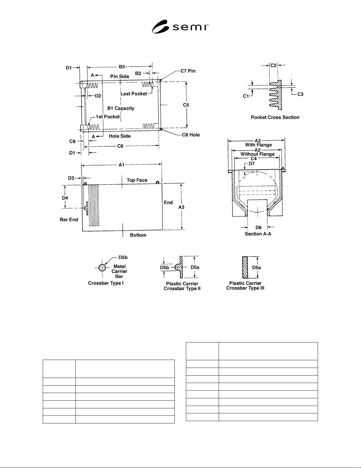
Table 1 Symbols Outline General Usage
Figure 1
Reference
Description
Overall Dimensions
A1 Length
A2 Width (with/without flange)
A3 Height (excluding pin)
Capacity
B1 Pockets per carrier
B2 Pocket spacing
B3 Center distance from the 1st to last pocket
Detail Dimensions
C1 Pocket width
C2 Pocket depth
C3 Pocket flat
C4 Pocket size
C5 Pin and hole location (width)
C6 Pin and hole location (length)
C7 Pin diameter and height
C8 Hole or slot
C9 Pin and hole center distance from pocket
center line
Machine Fit Specifications
D1 From the outside of the bar end to the
center line of the 1st pocket
D2 From the center line of the 1st pocket to the
closest point on the crossbar or web
D3 From the bar end of the carrier to the start
of the crossbar
D4 Center of the crossbar to the top face of the
carrier
D5 Crossbar specifications
D5a Bar web width on type II crossbar, or width
of the type III crossbar
D5b Bar width
D6 Track clearance
D7 Edge perimeter distance
Not shown — Wafer Tilt
SEMI E1-0697 © SEMI 1979, 2003 3
Figure 1
Wafer Carrier Outline — General Usage
NOTE: Used in conjunction with Table 1.
Table 2 Symbols Outline For Auto Transport Usage
Specifications
Figure 1A
Reference
Description
Overall Dimensions
A1 Length
A2a Width (with flange)
A2b Body width (measured at the crossbar)
A3 Height (excluding pin)
Capacity
Figure 1A
Reference
Description
B1 Pockets per carrier
B2 Pocket spacing (non-accumulative)
B3 Center distance from the 1st to last pocket
Detail Dimensions
C1 Pocket width
C2 Pocket depth
C3 Pocket flat
C4 Pocket size
SEMI E1-0697 © SEMI 1979, 2003 4
Figure 1A
Reference
Description
C5 Center of pin to center of hole
C6 Center pin to pin and hole to hole
C7
Diameter of pin (2×) times height of pin
C8 Diameter of hole
C9 Center of pin/hole to center of first pocket
Machine Fit Specifications
D1a From the outside plane of the bar end to
the center line of the 1st pocket opening
D1b Slot parallelism-coincident tolerance for
center line of slots
D2a From the center line of the 1st pocket to
the closest point on the crossbar or web
D2b From the center of the 25th pocket to the
closest point on the endwall
D3a The step from the bar end of the carrier to
the crossbar (the tolerance indicates
allowable bow)
D3b The step from the bar end of the carrier to
the crossbar (the tolerance indicates the
allowable deviation measured at a
maximum distance of 1/2" from the
crossbar/sidewall junction)
D4a From the bottom of the carrier to the
center of the crossbar, measured at the bar
end of the carrier
D4b From the bottom of the carrier to the
center of a nominal 125 mm wafer,
measured with wafer in place and carrier
sitting on bottom
D5a Bar web width which is the mass of
material which may be present on the
crossbar and is measured perpendicular to
the top surface
D5b Bar width measured perpendicular to the
top surface
D5c From the bar end of the carrier to the
surface of the bar web (the tolerance
indicates allowable bow)
D6a Track clearance which is the unobstructed
area between the two carrier sides on the
bar end and the distance between the two
sides at the bottom of the carrier for the
entire length of the carrier
D6b On the bar end surface, the distance
between the two struts perpendicular to the
crossbar
D6c On the bar end surface, the thickness of
each of the two struts perpendicular to the
crossbar
D6d On the bar end surface, the length of each
of the two struts
p
er
p
endicular to and
Figure 1A
Reference
Description
extending above the crossbar
D6e On the bar end surface, the length of each
of the two struts perpendicular to and
extending below the crossbar
D6f Radius allowed on the crossbar
D6g The overall width at the bottom of the
carrier measured within 3/8 inch from the
bottom
Wafer Tilt The allowable deviation of the wafer from
a parallel position in relation to the plane
of the bar end of the carrier, when said
wafer properly positioned and carrier is
resting on the bar end. Wafer is said to be
properly positioned when it is fully
inserted in pocket and is centered.
Wafer
Center
The allowable deviation of the center point
of the wafer from the center line to the
carrier (see Section A.A. Figure 5) when
carrier is resting on bottom and wafer is
fully inserted.
Detailed Dimensions
Handling Slots
D7
Dimensions
The handle slots are located on the bar end
and the opposite endwall of the carrier.
There are two slots on each end. These
slots are intended to be used as points for
engaging the carrier and picking it up.
Currently, these slots are used in both
manual and automated systems.
Dimensions D7a through D7d detail this
feature.
Pickup Flanges
D8
Dimensions
The pickup flanges are located on the
endwall of the carrier only. They are not
present on the bar end. There are two
flanges on the endwall. These flanges are
intended to be used for engaging the
carrier and picking it up. Currently, these
flanges are used in both manual and
automated systems. Dimensions D8a
through D8e detail this feature.
Center Alignment Features
D9
Dimensions
This feature is located on the bottom
sidewalls of the carrier. The center
alignment feature is used to find the
location of the first pocket. It is intended to
be used while the carrier is resting on its
bottom. This feature is used in conjunction
with wafer transfer machines and pick and
place equipment. Dimensions D9a through
D9k detail this feature.