semi合集-English.pdf - 第7427页
SEMI MF1529-1104 © SEMI 2004 8 contaminating material until sets of impressio ns can be made that do n ot exhibit fract ure. After a conditioni ng process, it is useful to clean the probe tip s with methanol on a cotton …

SEMI MF1529-1104 © SEMI 2004 7
Table 2 Nominal Values of the Standard Resistor
and of the Center-leg Resistor, r, for the Analog
Circuit Appropriate to Various Sheet Resistance
Range
#1
The resistance shall be within a range from one-half to twice the value listed
and its value shall be known to 0.05%.
8 Reagents and Materials
8.1 Purity of Reagents — All chemicals for which such
specifications exist shall conform to the assay and
impurity levels of Grade 1 SEMI specifications for
these specific chemicals. Other grades may be used,
provided it is first determined that the chemical is of
sufficiently high purity to permit its use without
lessening the accuracy of the test.
8.2 Purity of Water — Reference to water shall be
understood to mean Type E-3 or better deionized (DI)
water as described in ASTM Guide D 5127.
8.3 Qualification Wafers
8.3.1 Polished Silicon Wafers — Of any convenient
diameter for making probe impressions to be inspected
for general probe related damage and contact size and
shape. It is useful to divide the surface into rectangular
regions by use of scribe lines or similar technique to aid
in locating a particular series of impressions under the
inspection microscope.
8.3.2 One, or more, wafers from each of the processes
to be evaluated, for testing the electrical suitability of a
given probe for the intended evaluation.
8.4 Reagents for Surface Treatment — If surface
treatment is required, the following chemicals may be
needed:
8.4.1 Buffered HF — 10:1 or more dilute, in
accordance with SEMI C23.
8.4.2 2-Propanol — In accordance with SEMI C41.
8.4.3 Acetone — In accordance with SEMI C19.
8.4.4 Filtered dry nitrogen.
9 Sampling
9.1 In the case of referee measurements, it is left to the
parties to the test to agree upon the number of wafers
from a batch, and their selection procedure, as well as
the number and location of test positions on each wafer.
9.2 In the case of non-referee measurements, for
example, process control or research applications, it is
left to the user of this test method to determine the
number and location of test positions on each wafer.
10 Suitability of Test Specimen
10.1 The front and back surfaces of the wafer to be
measured should be tested for conductivity type using
Method A of SEMI MF42. If they are of the same
conductivity type, a thin sheet of insulating material,
such as mica, should be placed between the wafer and
the stage. This test is not necessary if the front and
back surfaces are known to be of opposite conductivity
type or if the layer is fully isolated from the substrate
by a dielectric layer.
10.2 If the wafer to be measured was fabricated by a
process that uses “finger” clamps or other types of
clamping that intrude into the top surface area of the
water, the wafer is unsuitable for use with sampling
plans that require measurements within several probe
spacings from the wafer perimeter.
11 Preparation of Apparatus
11.1 Visual Inspection of Probe Impressions — This
inspection should be performed when a new, rebuilt or
reconditioned probe is first installed to get an initial
indication of the mechanical performance of the probes.
Once a probe is installed, meets the visual inspection
criteria, and is left mounted, visual inspection of probe
impressions is generally not needed; functional probe
performance tests detailed in Section 11.2 generally
suffice to qualify the probe for continued use. Further
visual inspection of probe impressions is advised,
however, when a probe has trouble meeting the
requirements of Section 11.2.1. More routine
inspection of probe impressions is also advised if
probes are interchanged routinely for special
applications, thus increasing the risk of changes in the
alignment or rigidity of the probe mounting.
11.1.1 After selecting a probe for the intended
application, make a series of at least 10 probe
impressions on a polished silicon surface in steps of 50
to 125 m (0.002 to 0.005 in.). Examine the
impressions from each of the pins to determine that
there is no probe skidding, no cracks or fracture lines
surrounding any of the impressions, and that the
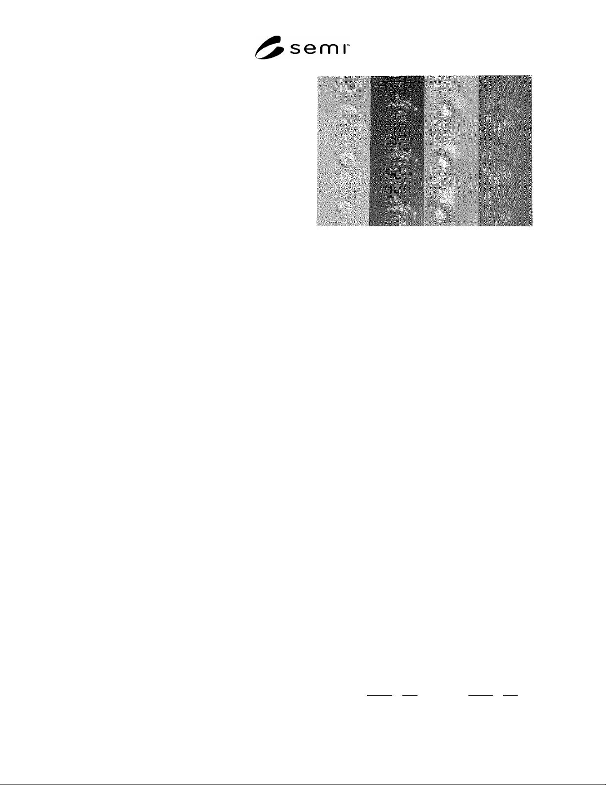
impressions are generally compact in nature (see Figure
3).
11.1.2 If fracture lines are seen, the probe must be
replaced, or conditioned on surfaces of ceramic,
sapphire, lapped silicon or other suitable, non-
Sheet Resistance,
Analog and Standard
Resistor,
#1
<2.5 1
2–25 10
20–250 100
200–2,500 1,000
2,000–25,000 10,000
SEMI MF1529-1104 © SEMI 2004 8
contaminating material until sets of impressions can be
made that do not exhibit fracture. After a conditioning
process, it is useful to clean the probe tips with
methanol on a cotton swab to loosen debris that may
have collected in the tip.
11.1.3 If probe skidding is seen, tighten or otherwise
adjust the probe clamp and probe lowering mechanism
to eliminate skidding.
11.1.4 If non-compact probe impressions are seen,
acceptable data may result, but the probe tip(s) are
generally in an advanced state of wear and may not be
stable with use.
11.2 Probe Performance Verification — This test must
be performed before any series of referee
measurements, or if a type of layer is being measured
for which there is not past experience regarding proper
selection of probe radius, load and conditioning. It
qualifies a probe for taking highly repeatable
measurements, as are needed for mapping spatial
variations of sheet resistance, but does not ensure
accuracy of measured value. It should be performed
separately for each type of layer to be measured.
11.2.1 Select a wafer of the type to be checked for
uniformity. At five different locations that are
reasonably well separated on the wafer, make a series
of 10 measurements following the procedure of
Sections 12.4 to 12.6, 13.1, and 13.2, using steps no
larger than 100 m between each of the 10
measurement positions. Calculate the average and
standard deviation for each of the five sets of
measurements. For a probe to be satisfactory for use in
measuring layers of this type, the standard deviation
must be no more than 0.1% of the average for at least
four of these sets.
11.3 Qualification of Measurement Electronics — The
suitability and accuracy of the measurement electronics
shall be verified immediately prior to a referee
measurement unless the equipment is separately
demonstrated to be under statistical control for
measurements of that process. For non-referee
applications, use of the analog circuits is helpful for
troubleshooting or performance monitoring of the
electronics.
11.3.1 Analog Test Circuit
11.3.1.1 With the current supply short-circuited or
turned off, attach the current leads from the analog test
circuit of the appropriate resistance value to the current
supply and connect the potential leads designated V (see
Figure 2) from the analog circuit to the input of the
voltage measuring instrumentation. Allow sufficient
time for the electronics to warm up in accordance with
the manufacturers instructions.
a b c d
#1
All probe impressions were made with steps of about 50
m between impressions, and using probes loaded more
heavily than would normally be done for measuring thin
films; this was done to provide better photographic detail.
Figure 3
Photographs of Three Indentations Each from (a) a
Satisfactory Probe Tip, (b) a Badly Worn Probe Tip,
(c) a Probe Tip Causing Conchoidal Fracture, (d) a
Probe Tip Showing Skidding
NOTE 8: Caution: Constant-current power supplies often
operate at output voltages of several hundred volts when not
connected to a load. Any changes of connection to a
constant-current supply should be made either with the
current supply turned off or with its output short-circuited.
11.3.2 With the current initially in either direction (to
be called “forward”) adjust its value to give a measured
voltage of between 7 and 12 mV (see Table 1 for
nominal values). Record the current, I
f
, through the
analog box, or measure the potential, V
sf
, across the
appropriate standard resistor connected in series with
the analog box. Measure the potential, V
af
, across the
analog box. Reverse the direction of the current and
record the current, I
r
, or measure the potential V
sr
,
across the standard resistor; measure the potential, V
ar
,
across the analog box. Repeat this procedure until ten
sets of data have been taken. All values measured and
recorded must be known to at least four significant
figures.
11.3.3 Calculations for the Analog Test Circuit
11.3.3.1 Calculate the resistance of the analog box
resistor for both forward and reverse directions of
current using the appropriate form of the equations
according to whether, or not, a standard resistor was
used as follows:
ar
ar
sr
sar
r
af
af
sf
saf
f
I
V
V
RV
r
I
V
V
RV
r and (1)

SEMI MF1529-1104 © SEMI 2004 9
where:
r
fi
and r
ri
= the calculated values for the analog box
resistor, with current in the forward an
d
reverse directions, respectively, for the
i
th
measurement,
R
s
=
the value of the standard resistor, ,
V
af
and V
ar
= the potentials measured across the
analog box in the forward and reverse
directions, respectively,
I
af
and I
ar
= the values of the current in the forward
and reverse directions, and
V
sf
and V
sr
= the potentials measured across the
standard resistor in the forward an
d
reverse directions.
11.3.3.2 For each of the ten pairs, r
fi
and r
ri
, calculate
the average, r
mi
:
)(
2
1
rifimi
rrr (2)
11.3.3.3 Calculate the overall average,
m
r
v
of these ten
values of r
mi
:
10
1
10
1
i
mim
rr
v
(3)
11.3.3.4 Calculate the sample standard deviation, s
a
, of
the ten values as follows:
10
1
2
3
1
i
mmia
rrs
v
(4)
11.3.4 Requirements for the Analog Test Circuit — For
the electrical equipment to be suitable for referee
measurements at the sheet resistance value just
simulated, it must meet the following requirements:
11.3.4.1 The value of
m
r
v
must be within 0.25% of the
known value of the resistor, r, and
11.3.4.2 The value of the standard deviation, s
a
must be
no greater than 0.1% of
m
r
v
.
NOTE 9: If not previously known, the value of the analog
circuit resistor may be determined by using the procedure of
Sections 11.3.1 to 11.3.3.2 but measuring the potential across
the analog box using the connections V in Figure 2.
12 Procedure
12.1 Specimen Preparation
12.1.1 If the specimens have been kept in a clean, non-
contaminating atmosphere, or are to be measured within
3 h after fabrication, proceed to Section 12.2.
12.1.2 Remove possible organic contaminants that may
arise from the storage container as follows: Rinse the
specimen in acetone for 1 min. Remove. Immediately
immerse in 2-propanol for 1 min. Remove. Blow dry
with filtered dry nitrogen. Repeat if necessary until
specimen is free from visible stains, streaking or other
visual evidence of residue.
12.2 Mounting and Checking the Wafer
12.2.1 Using vacuum paddle, tweezers, or robotic
arrangement, mount the wafer on the stage, so that the
wafer center is within 1 mm of the stage center. Clamp
the wafer to the stage with vacuum or other means.
Lower the probes onto the wafer. If not known
measure the electrical resistance between any of the
probe pins and the stage to verify that the electrical
isolation is at least 10
9
.
12.2.2 Allow sufficient time for the wafer's temperature
to equilibrate with that of the stage. Thirty seconds is
sufficient if the wafer had been held at room
temperature prior to mounting. Longer times are
necessary if the wafer was recently removed from a
reactor or other elevated temperature process.
NOTE 10: The absolute value of the wafer temperature
during measurement affects the absolute values of sheet
resistance, particularly for lightly doped layers, but it should
not affect the measurement of uniformity of sheet resistance
values, as long as the temperature is constant within 0.2°C
during measurement of any wafer. However, for referee
measurements or process control applications, for which the
absolute sheet resistance values are likely to be an important
part of the measurement results, it is important to maintain the
stage temperature within a narrow range (e.g., 23 ± 1°C) or to
develop an empirical relation between sheet resistance and
measurement temperature for each layer fabrication process
of interest.
12.3 Measurement Site Selection — Using the
measurement site selection agreed to for a referee
measurement or that decided upon for process control
or other application, follow Sections 12.4 through 12.6
at each measurement site before raising the probe and
moving to the next site.
NOTE 11: Various site selection plans may be chosen
according to the application needs. These include, but are not
limited to: diameter scans with step sizes appropriate to the
spatial resolution needed, sparse sampling extensions of the 5-
point and 9-point plans described in SEMI MF81, and area
sampling plans with the size of the area and number of points
chosen by measurement time constraints and process
information requirements, such as the circular or rectangular
patterns of SEMI MF1618. This test method makes no
recommendation about choice of sampling plans, since user
needs and interests are widely varied.
NOTE 12: If wafer diameter scans are chosen, the probe
should not be oriented so that the pins lie exactly along the