semi合集-English.pdf - 第7479页
SEMI MF1618-1104 © SEMI 2004 9 Table A1-2 Approximate Nu mber of Measurement Sites for Various Numbers of Row s and Columns in a Cartesian Sampling Plan Number of rows and columns 7 9 11 13 15 17 Number of sites 37 69 97…
SEMI MF1618-1104 © SEMI 2004 8
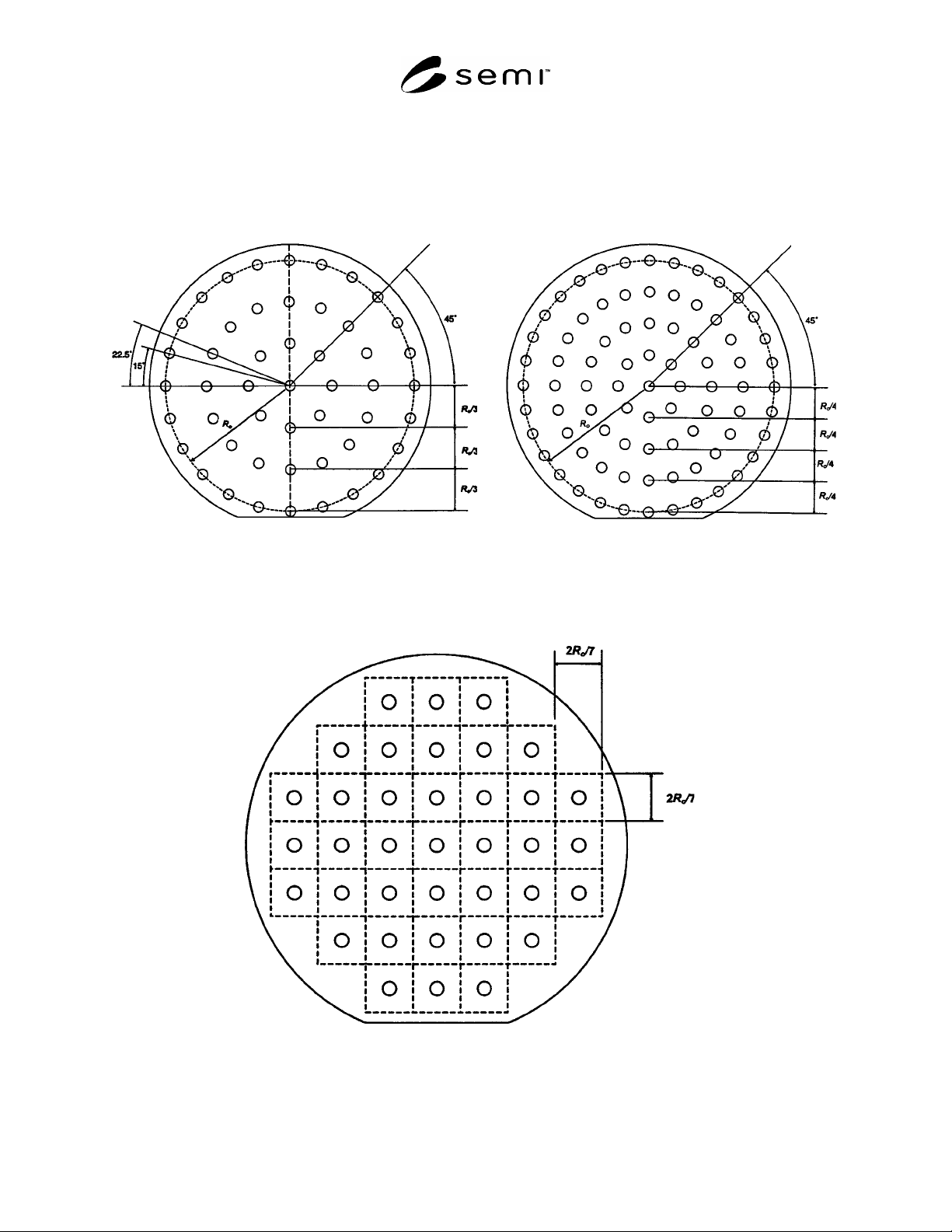
made, and the amount of information desired about the uniformity of the thin film. The square cells in this plan are
not necessarily the shape or size of the sampling area for the measurement being used. In general, make sure that
the sampling area for the measurement is smaller than the dimensions of the square.
(a) Three-circle Case (b) Four-circle Case
NOTE: The radius R
o
is given by Equation A1-1 for Method A and by Equation A1-2 for Method B.
Figure A1-2
Illustrations of Concentric Circle Sampling Plans
NOTE: The radius R
o
as discussed in A1-1.1 is not shown in this figure.
Figure A1-3
Illustration of the Cartesian Measurement Site Plan for the Case of Seven Rows by Seven Columns
SEMI MF1618-1104 © SEMI 2004 9
Table A1-2 Approximate Number of Measurement
Sites for Various Numbers of Rows and Columns in
a Cartesian Sampling Plan
Number of
rows and
columns
7 9 11 13 15 17
Number of
sites
37 69 97 137 177 225
A1-4.3 The size of the cells, and the separation of the
measurement sites along the x- and y-axes, is
determined by the number of rows and columns into
which the wafer surface is partitioned. Use Table A1-2
as a guide to the approximate number of measurement
sites for various numbers of rows and columns of cells.
To calculate the dimensions of the square cells, divide
the outermost radius, R
o
, determined in Section A1.1,
by N, the desired number of rows and columns. The
exact number of sites that will be measured is governed
by the number of cells near the wafer perimeter that
need to be excluded because the center of the cell, that
is, the center of the measurement spot, does not fall
within the radius R
o
.
A1-4.4 Use test instrument software to establish the
coordinates of the center of all cells as determined from
the ratio R
o
/N
C
, calculated in Section A1-4.3. Disallow
measurement sites near the wafer perimeter such that
the radial distance to the center of the cell, that is, the
center of the measurement spot, is larger than R
o
. This
follows the same rationale for allowed measurement
sites as is used with the concentric circle plans.
A1-4.5
Take measurements at all sites allowed in
accordance with Table A1-2. The measurement
sequence, whether starting from the center point and
moving outward or starting from one edge a row or
column at a time, is to be decided by the parties to the
test.
A1-4.6
Calculate the uniformity based on the difference
between the maximum and minimum measured values,
HLV(%), and on the standard deviation as a percent of
the mean of all measurements, SUP(%), as detailed in
Section 9.3.
A1-5 Single-Diameter Sampling Plan
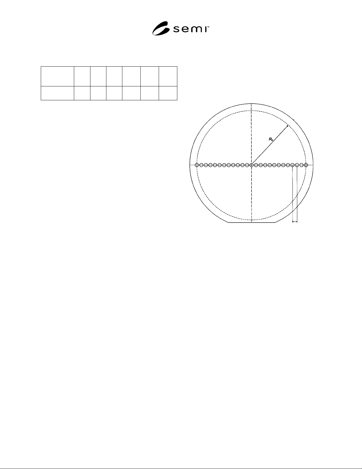
A1-5.1 This plan uses a very high density of
measurements along a diameter and includes a
measurement at the wafer center. It is shown
schematically in Figure A1-4 for the diameter being
parallel to a major wafer flat. However, in the case of
notched wafers, the notch would replace the flat in the
figure. It is also possible, by agreement of the parties to
the test, to make the measurements along a diameter at
a specified angle with respect to the fiducial axis as
long as such an angle is then stated in the report.
A1-5.2
Choose a value, N
M
, for the number of
measurements, where N
M
is at least 25. The separation
between measurement sites is given by 2R
o
/(N
M
1),
where R
o
is determined as in Section A1-1.1.
2R
o
/(N
M
–1)
NOTE: The radius R
o
is given by Equation A1-1 for Method
A and by Equation A1-2 for Method B.
Figure A1-4
Illustration of Single-Diameter, High-Density
Measurement Site Plan
A1-5.2.2 Compare the site separation, 2R
o
/(N
M
1),
with the estimated measurement sampling area or spot
size. If the interval is smaller than this value, little
additional information may be obtained by choosing so
large a value for N
M
; it may be appropriate to reduce N
M
so that the new calculated site separation is equal to or
greater than the measurement sampling area.
A1-5.3
Establish the coordinates for all measurement
sites using the site interval value just calculated and the
wafer center as the reference point. Take
measurements at all sites.
A1-5.4
Calculate the uniformity based on the difference
between the maximum and minimum measured values,
HLV(%), and on the standard deviation as a percent of
the mean of all measurements, SUP(%), as detailed in
Section 9.3.

SEMI MF1618-1104 © SEMI 2004 10
NOTICE: SEMI makes no warranties or
representations as to the suitability of the standards set
forth herein for any particular application. The
determination of the suitability of the standard is solely
the responsibility of the user. Users are cautioned to
refer to manufacturer’s instructions, product labels,
product data sheets, and other relevant literature,
respecting any materials or equipment mentioned
herein. These standards are subject to change without
notice.
By publication of this standard, Semiconductor
Equipment and Materials International (SEMI) takes no
position respecting the validity of any patent rights or
copyrights asserted in connection with any items
mentioned in this standard. Users of this standard are
expressly advised that determination of any such patent
rights or copyrights, and the risk of infringement of
such rights are entirely their own responsibility.
Copyright by SEMI® (Semiconductor Equipment and Materials
International), 3081 Zanker Road, San Jose, CA 95134. Reproduction
of the contents in whole or in part is forbidden without express
written consent of SEMI.