semi合集-English.pdf - 第5466页
SEMI PR9-0705 © SEMI 2005 10 (A) Package with Shut-off Valve and Mas s Flow Controller (B) Panel in Enclosur e Consistency of Six Packages. Applications Include Gas Chromatography, Analytical Instrume ntation, Semiconduc…
SEMI PR9-0705 © SEMI 2005 9
9.4.9 Test for shock and vibration. Check for operation and leak integrity before and after testing. MIL-STD 810
9.4.10 Test for performance at maximum and minimum voltages based on product specifications.
9.4.11 Perform electrical testing and validation. Check for power consumption, response time, noise, dielectric
breakdown, resistance fluctuations, others?
9.4.12 Test for compatibility with typical, operating and/or specified fluids for validation testing.
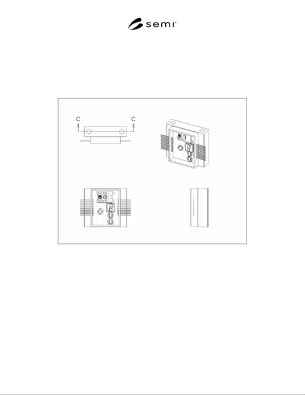
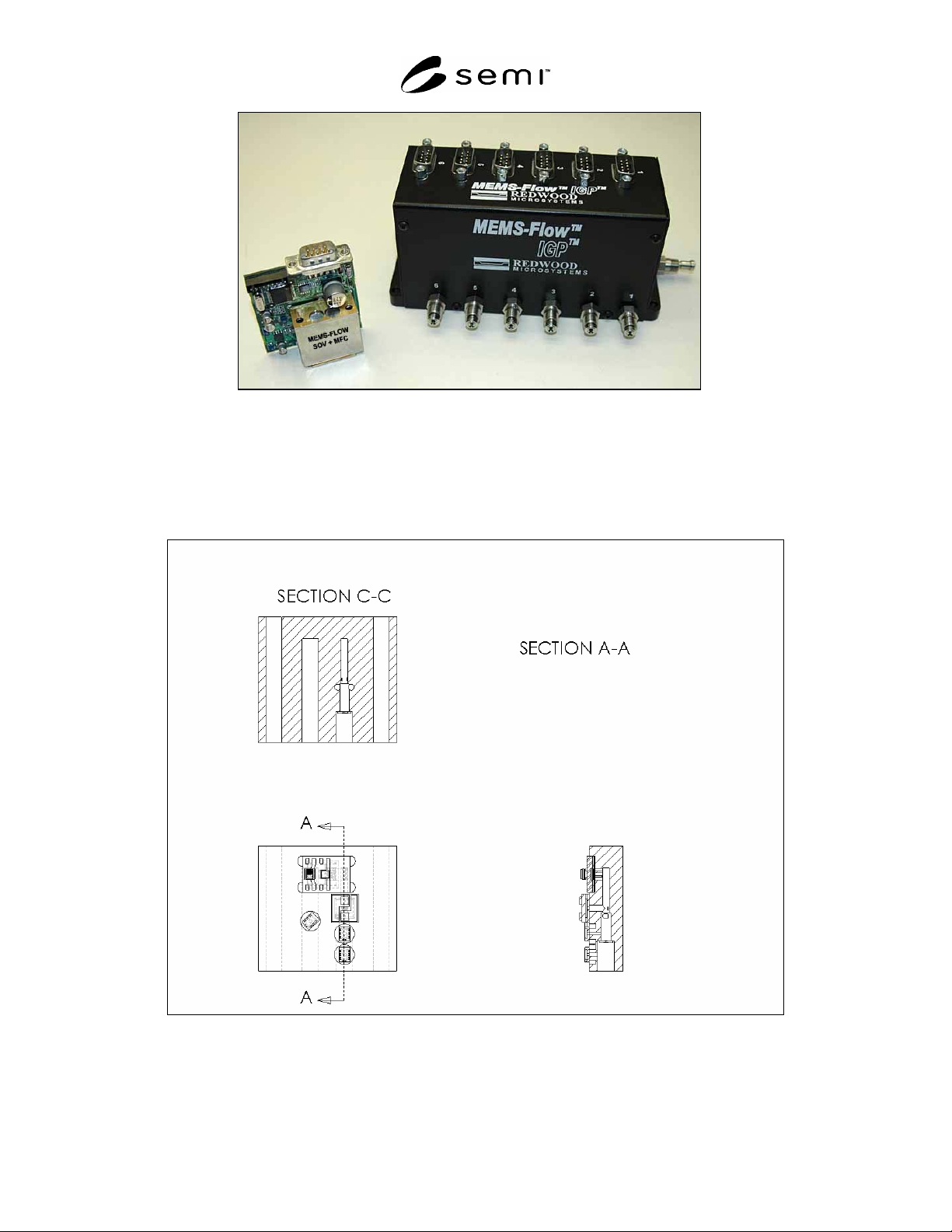
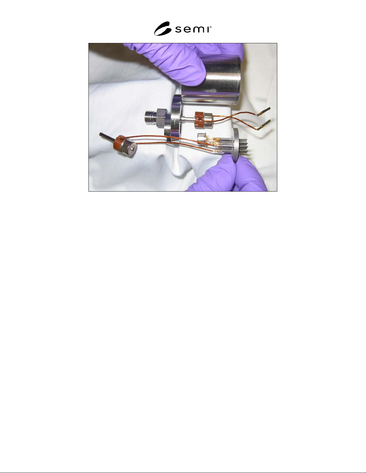
9.4.12.1 See Figures 1–4 of a MEMS System with subsystem fluidic interface features.
9.4.12.2 Courtesy Redwood MicroSystems
Figure 1
Mechanical Drawing Showing MEMS System
SEMI PR9-0705 © SEMI 2005 10
(A)
Package with Shut-off
Valve and Mass Flow Controller
(B)
Panel in Enclosure Consistency of Six
Packages. Applications Include Gas
Chromatography, Analytical
Instrumentation, Semiconductor
Processing.
Figure 2
Figure 3
Mechanical Drawing Showing MEMS Subsystem and Fluidic Adaptor
SEMI PR9-0705 © SEMI 2005 11
Figure 4
Microvalve in Fusion Reactor
9.5 Purpose — To be developed.
9.6 Scope — To be developed.
NOTICE: SEMI makes no warranties or representations as to the suitability of the standards set forth herein for any
particular application. The determination of the suitability of the standard is solely the responsibility of the user.
Users are cautioned to refer to manufacturer's instructions, product labels, product data sheets, and other relevant
literature, respecting any materials or equipment mentioned herein. These standards are subject to change without
notice.
By publication of this standard, Semiconductor Equipment and Materials International (SEMI) takes no position
respecting the validity of any patent rights or copyrights asserted in connection with any items mentioned in this
standard. Users of this standard are expressly advised that determination of any such patent rights or copyrights, and
the risk of infringement of such rights are entirely their own responsibility.
Copyright by SEMI® (Semiconductor Equipment and Materials
International), 3081 Zanker Road, San Jose, CA 95134. Reproduction of
the contents in whole or in part is forbidden without express written
consent of SEMI.