semi合集-English.pdf - 第7908页
SEMI T14-1104 © SEMI 2004 5 6.0 µ m +10% -20% +10% -20% Figure 3 Dot Shape Circle (Projected Sectional Area) To Waf er Center Reference Poin t The Prima ry Border R ow The Primary B order Colu mn Figure 4 Data Matrix Cod…
SEMI T14-1104 © SEMI 2004 4
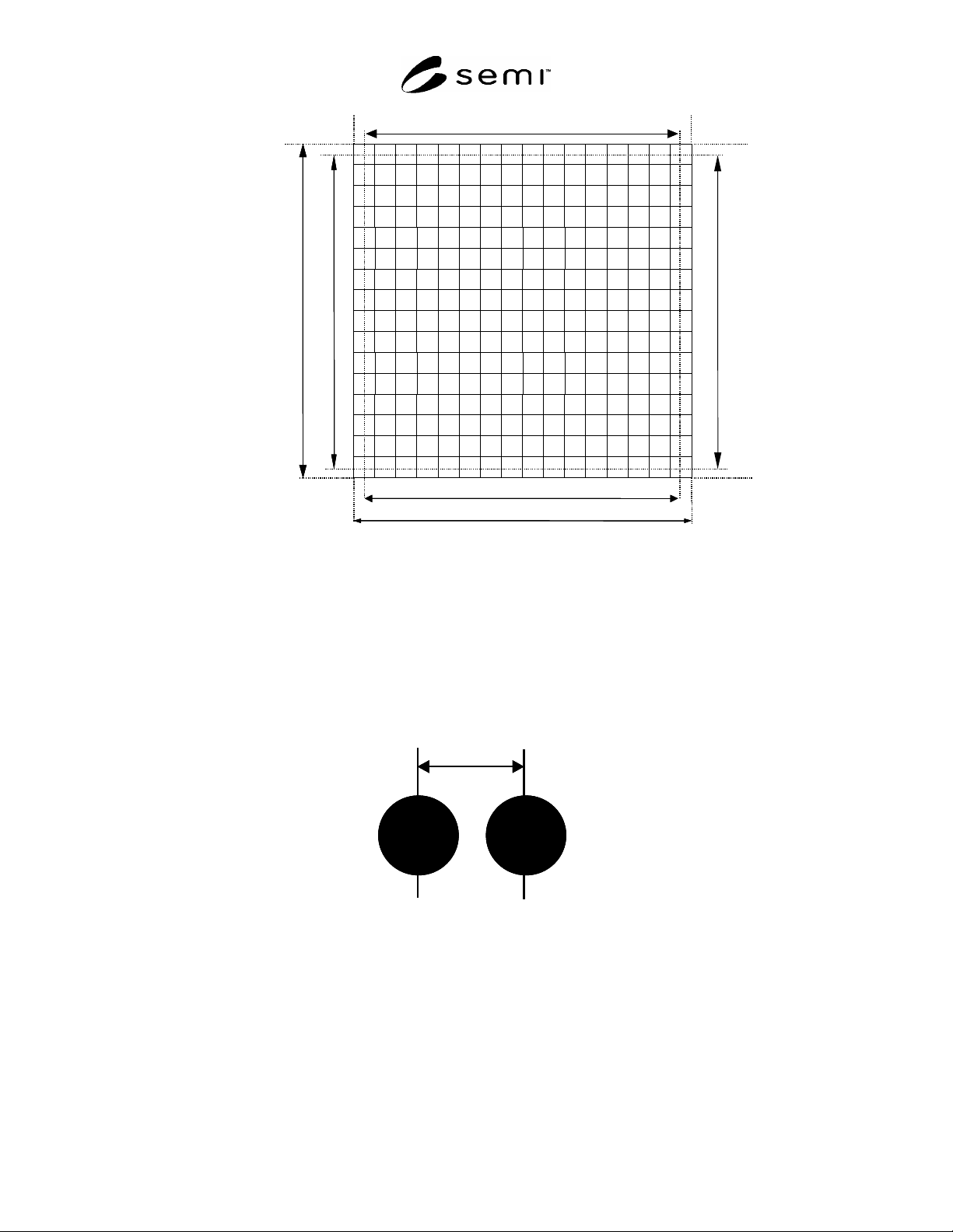
Nominal Dimensions (µm)
R1 = 92.00 ± 6%
C2 = 98.00 ± 6% R2 = 98.00 ± 6%
C1 = 92.00 ± 6%
16
cells per row
C1
C2
R1
R2
16
cells per
column
C
L
C
L
C
L
C
L
16
cells per row
C1
C2
R1
R2
16
cells per
column
C
L
C
L
C
L
C
L
C
L
C
L
C
L
C
L
Figure 1
Data Matrix Field Dimensions
ECC200 - 16 rows × 16 columns
6.25 µ m
6.25
µ
m
Figure 2
Cell Spacing
SEMI T14-1104 © SEMI 2004 5
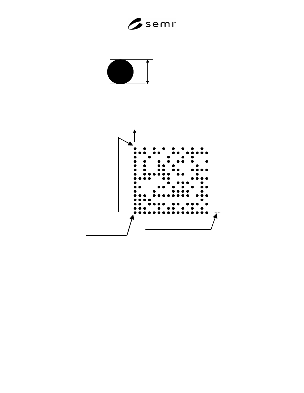
6.0 µm
+10%
-20%
+10%
-20%
Figure 3
Dot Shape Circle (Projected Sectional Area)
To Wafer Center
Reference Point
The Primary Border Row
The Primary Border Column
Figure 4
Data Matrix Code Fields
ECC200 - 16 rows × 16 columns
SEMI T14-1104 © SEMI 2004 6
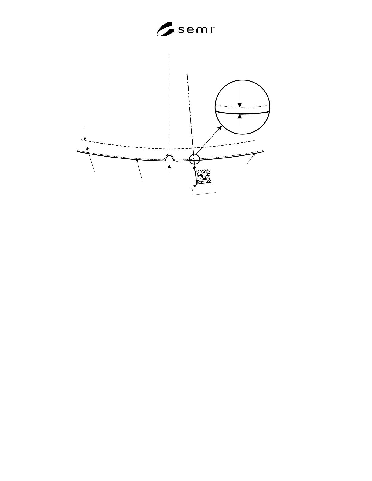
Orientation Fiducial Axis
[011]
Notch
WAFER SURFACE
3.0 from
Orientation Fiducial Axis
Outer periphery of FQA
Edge Exclusive Area
Edge Profile region
Wafer Periphery
Orientation Fiducial Axis
[011] ± 1.0°
Notch
WAFER SURFACE
3.0 ± 0.1° from
Orientation Fiducial Axis
Outer periphery of FQA
Edge Exclusive Area
Edge Profile region
Wafer Periphery
R
e
f
e
r
e
n
c
e
P
o
i
n
t
ID Mark Area
NOTE: Figure 5 is not to scale.
Figure 5
Data Matrix Code Location on Front Bevel Surface of Notched 300 mm Diameter Wafer
Top View