semi合集-English.pdf - 第7413页
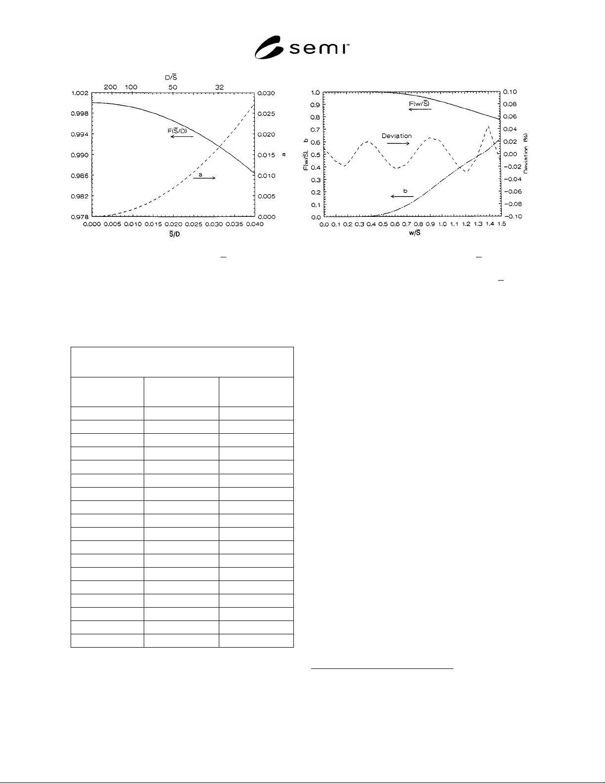
SEMI MF1527-1104 © SEMI 2003, 2004 19 Figure R2-1 Figure R2-2 Diameter Correction Factor, F ( S /D ), and Thickness Correction Factor, F ( w / S ), Error Error Coeffici ent, a Coefficient, b , and Percentage Deviation be…
SEMI MF1527-1104 © SEMI 2003, 2004 18
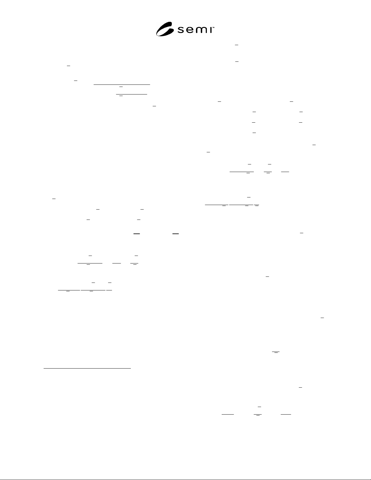
R2-3.1 Diameter Correction Factor—For measure-
ments at the center of a circular wafer, this factor is
given as a function of the ratio of the average probe-tip
spacing, S , to the diameter, D, as follows:
15
3)/(
3)/(
ln2ln
2ln
)/(
2
2
DS
DS
DSF
(R2-5)
This factor is plotted in Figure R2-1 for
S /D ratios
from 0 to 0.04, which includes all practical ratios for
wafers of diameter 50.8 mm (2.00 in.) and up for
probes with average probe-tip spacing of 0.635 mm
(0.025 in.) to 1.588 mm (0.0625 in.). These ratios
range from 0.00212 for a 300-mm diameter wafer and a
probe-tip spacing of 0.635 mm to 0.03125 for a 50.8-
mm diameter wafer and a probe-tip spacing of 1.588
mm.
R2-3.1.1 Over this range, the factor can be fitted to
better than 0.001% with the following fourth-order
polynomial:
53
25
)/(841714.70)/(181781.0
)/(657959.8)/(104887.1
000000.1)/(
DSDS
DSDS
DSF
(R2-6)
R2-3.1.2 The effect of variation in S or D on F ( S
/D) is given as follows:
S
S
a
D
D
a
DS
DSF dd
)/(F
)/(d
(R2-7)
where:
D
S
DS
DSF
DSF
a
)/(
)/(
)/(
1
R2-3.1.3 The coefficient, a, is also plotted in Figure
R2-1. It is sufficiently small that this source of error
can be neglected in all practical cases.
R2-3.2 Thickness Correction Factor—This factor is a
slowly converging infinite series that was tabulated by
Smits
15
based on a calculation method developed by
Uhlir.
16
A relatively efficient formula
17
for calculating
15 Smits, F. M., “Measurement of Sheet Resistivities with the Four-
point Probe,” Bell Sys. Tech. J. 37, 711–718 (1958).
16 Uhlir, A., Jr., “The Potentials of Infinite Systems of Sources and
Numerical Solutions of Problems in Semiconductor Engineering,”
Bell Sys. Tech. J. 34, 105–127 (1958)
17 Phillips, W. E., “Correction Factor for Finite Thickness,” in
Methods of Measurement for Semiconductor Materials, Process
Control and Devices: Quarterly Report, October 1 to December 31,
1970, NBS Technical Note 592, W. M. Bullis, Ed., August 1971, pp.
9–11. Available from the National Technical Information Service,
Springfield, VA 22161, as AD 728611.
this factor,
)/( SwF , is given in Related Information 1
of SEMI MF84; the result is plotted in Figure R2-2 over
the range of
Sw/ from 0 to 1.5, which covers all
practical measurements of standard sized wafers as
specified in SEMI M1. Over this range, the factor may
be approximated to better than ±0.04% by a sixth-order
polynomial as follows:
6
54
32
)/(154327.0
)/(684549.0)/(001842.1
)/(461693.0)/(069677.0
)/(001130.0000107.1)/(
Sw
SwSw
SwSw
SwSwF
(R2-8)
R2-3.2.1 The effect of variations in w or
S on
)/( SwF is given as follows:
w
w
b
S
S
b
SwF
SwF dd
)/(
)/(d
(R2-9)
where:
.
)/(
)/(
)/((
1
S
w
Sw
SwF
SwF
b
R2-3.2.2 The coefficient, b, is also plotted in Figure
R2-2 together with the percent deviation of the
polynomial fit (Eq. R2-8) from
)/( SwF . The
oscillations due to the polynomial fit can be seen in the
plots of both b and the percent deviation. However, the
curve for b calculated from the derivative of the
polynomial fit provides a reasonable estimate of its
magnitude. It can be seen that the coefficient, b,
becomes rather large when w/ S is greater than about 1
that occurs when large diameter wafers (w 0.625 mm)
are measured with a four-point probe with probe
spacing of 0.635 mm (0.025 in.).
R2-3.3 Probe-Tip Spacing Correction Factor—When
the probe-tip spacings differ from their mean value,
S ,
by only a few percent, this factor is given
approximately as follows:
14
S
S
F
sp
2
1082.11 (R2-10)
where:
S
2
= the spacing between the inner two probes, mm.
R2-3.3.1 The effect of variations in S
2
or
S on F
sp
is
given as follows:
2
2
d
082.1
d
082.1
d
S
S
S
S
F
F
sp
sp
(R2-11)
SEMI MF1527-1104 © SEMI 2003, 2004 19
Figure R2-1 Figure R2-2
Diameter Correction Factor, F(
S /D), and Thickness Correction Factor, F(w/ S ), Error
Error Coefficient, a Coefficient, b, and Percentage Deviation
between Fit (Equation R2-7) and F(w/
S )
R2-3.3.2 Uncertainty in probe-tip spacing arises both
from the error in measurement and from probe-tip
wander.
R2-4 Temperature Correction Factor—SEMI MF84
requires that the resistivity of a silicon wafer be
corrected to its value at 23°C. Between 18° and 28°C,
the resistivity of silicon can be treated as a linear
function of the temperature; over this temperature
range, the temperature correction factor, F
T
is given as
follows:
)23(1
TCF
TT
(R2-12)
where:
C
T
= temperature coefficient of resistivity,
(·cm)/(·cm·°C), and
T = temperature, °C, at which the resistivity
measurement was made.
R2-4.1 The temperature coefficient has been deter-
mined experimentally as a function of the resistivity of
both boron- and phosphorus-doped silicon.
18
As
outlined in SEMI MF84, the experimental data have
been fitted with polynomials of the form:
k
n
n
nT
AC
0
)(ln
(R2-13)
where:
A
n
= the appropriate coefficients (see Table R2-1),
=
wafer resistivity, ·cm, and
k = 17 for phosphorus-doped silicon and 13 for boron-
doped silicon.
R2-4.2 These polynomials are such that nowhere
within the resistivity range 0.001 and 500 ·cm does
the value of C
T
derived from them deviate from the
18 Bullis, W. M., Brewer, F. H., Kolstad, C. D., and Swartzendruber,
L. J., “Temperature Coefficient of Resistivity of Silicon and
Germanium Near Room Temperature,” Solid-State Electron. 11, 639–
646 (1968).
Table R2-1 Polynominal Coefficients for
Temperature Coefficient of Resistivity, %/°C
Coefficient
Phosphorus-Doped
Silicon
Boron-Doped
Silicon
A
0
7.364 × 10
1
7.068 × 10
1
A
1
6.560 × 10
2
8.544 × 10
2
A
2
3.075 × 10
2
1.478 × 10
2
A
3
2.427 × 10
3
1.635 × 10
3
A
4
7.5883 × 10
3
2.003 × 10
3
A
5
7.5541 × 10
4
3.415 × 10
4
A
6
1.39760 × 10
3
2.0915 × 10
4
A
7
1.159 × 10
6
4.3237 × 10
5
A
8
1.106882 × 10
4
7.0532 × 10
6
A
9
4.56719 × 10
6
1.60868 × 10
6
A
10
4.407686 × 10
6
1.0346 × 10
7
A
11
2.601512 × 10
7
2.5201 × 10
8
A
12
9.408560 × 10
8
5.6419 × 10
10
A
13
6.190700 × 10
9
1.4445 × 10
10
A
14
1.032377 × 10
9
A
15
6.890181 × 10
11
A
16
4.58514 × 10
12
A
17
2.94332 × 10
13
SEMI MF1527-1104 © SEMI 2003, 2004 20
curve drawn through the experimental data
18
by more
than 0.0002 (·cm)/(·cm·°C). SEMI MF84 includes a
table of values calculated from this fit and extended
down to 0.0006 ·cm and up to 100 ·cm by taking
smoothed values to avoid the oscillations of the
polynomials in the extreme regions.
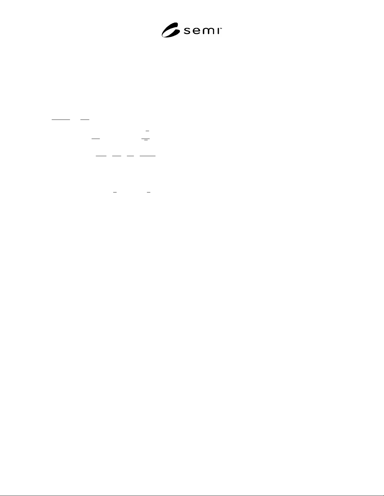
R2-5 By substituting these relations into Equation R2-
4, one obtains the following:
T
T
C
C
F
TC
I
I
V
V
S
S
S
S
ba
w
w
b
D
D
a
d
dd
d
082.1
d
)082.1(
d
)1(
d
d
2
2
23
23
(R2-14)
R2-6 Estimates of the errors in resistivity measurement
due to uncertainties in diameter, thickness and probe-tip
spacing can be made by inserting the values of a and b
appropriate to the ratios
S
/D and w/
S
from Figure
R2-1 and Figure R2-2 into Equation R2-14.
R2-7 It should also be emphasized that uncertainties
due to lateral and axial resistivity inhomogeneity in the
reference wafer are likely to cause significant errors in
resistivity measurement that may be as large or larger
than those discussed in this appendix unless the
material for the reference wafers is carefully selected
for the best possible uniformity.
NOTICE: SEMI makes no warranties or
representations as to the suitability of the standards set
forth herein for any particular application. The
determination of the suitability of the standard is solely
the responsibility of the user. Users are cautioned to
refer to manufacturer's instructions, product labels,
product data sheets, and other relevant literature,
respecting any materials or equipment mentioned
herein. These standards are subject to change without
notice.
By publication of this standard, Semiconductor
Equipment and Materials International (SEMI) takes no
position respecting the validity of any patent rights or
copyrights asserted in connection with any items
mentioned in this standard. Users of this standard are
expressly advised that determination of any such patent
rights or copyrights, and the risk of infringement of
such rights are entirely their own responsibility.
Copyright by SEMI® (Semiconductor Equipment and Materials
International), 3081 Zanker Road, San Jose, CA 95134. Reproduction
of the contents in whole or in part is forbidden without express
written consent of SEMI.