semi合集-English.pdf - 第6276页
SEMI G54-93 © SEMI 1993 4 8 Packaging and M arking 8.1 Packagi ng — Tooling m u st be p a cked in contain ers designed and constructed to prov ide protection against normal transportation d amage risks and spillage. The …
SEMI G54-93 © SEMI 19933
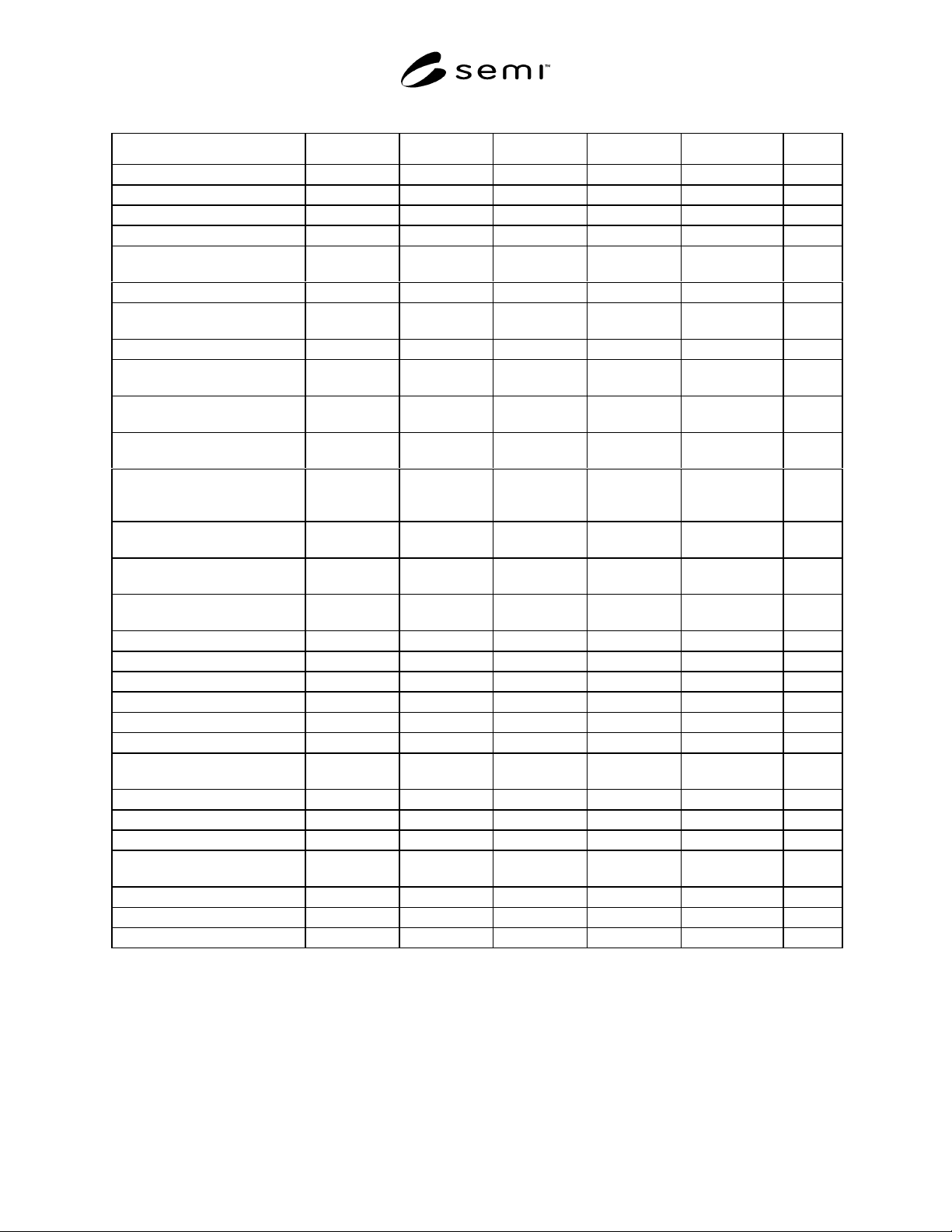
Table 1 Tolerance Limits
Dimension (Tolerance) PDIP PLCC SOIC PQFP PTAB UNITS
Package Length/Width ± 0.002 (0.05) 0.002 (0.05) 0.002 (0.05) 0.002 (0.05) 0.002 (0.05) in. (mm)
Cavity Mismatch ± 0.002 (0.05) 0.002 (0.05) 0.002 (0.05) 0.002 (0.05) 0.002 (0.05) in. (mm)
Cavity Overlap (Max.) 0.002 (0.05) 0.002 (0.05) 0.002 (0.05) 0.002 (0.05) 0.002 (0.05) in. (mm)
Package/Leadframe Offset ± 0.002 (0.05) 0.002 (0.05) 0.002 (0.05) 0.002 (0.05) 0.001 (0.025) in. (mm)
Plastic Body Thickness —
Top and Bottom ±
0.002 (0.05) 0.002 (0.05) 0.002 (0.05) 0.002 (0.05) 0.001 (0.025) in. (mm)
Surface Protrusions (Max.) 0.001 (0.025) 0.001 (0.025) 0.001 (0.025) 0.001 (0.025) 0.001 (0.025) in. (mm)
Surface Intrusions —
Depth (Max.)
0.001 (0.025) 0.001 (0.025) 0.001 (0.025) 0.001 (0.025) 0.001 (0.025) in. (mm)
-X-Y Dimension (Max.) 0.010 (0.25) 0.010 (0.25) 0.010 (0.25) 0.010 (0.25) 0.005 (0.127) in. (mm)
Ejector Pins — Intrusion only
(Max.)
0.010 (0.25) 0.010 (0.25) 0.010 (0.25) 0.008 (0.20) 0.005 (0.127) in. (mm)
Gate Feature — Intrusion only
(Max.)
0.020 (0.50) 0.020 (0.50) 0.010 (0.25) 0.020 (0.50) 0.002 (0.05) in. (mm)
Gate Feature — Protrusion only
(Max.)
0.004 (0.10) 0.004 (0.10) 0.004 (0.10) 0.004 (0.10) 0.004 (0.10) in. (mm)
Parting Line Protrusion — after
deflash dambar removal
(Max. per side)
0.006 (0.15) 0.006 (0.15) 0.006 (0.15) 0.006 (0.15) 0.005 (0.127) in. (mm)
Parting Line Intrusion —
Plastic (Max.)
0.010 (0.25) 0.010 (0.25) 0.005 (0.127) 0.010 (0.25) 0.005 (0.127) in. (mm)
Parting Line Protrusion —
after package singulation
0.006 (0.15) 0.006 (0.15) 0.006 (0.15) 0.006 (0.15) 0.005 (0.127) in. (mm)
Warp Factor (Max.) —
up to a Limit of
2.5% 0.003
(0.08)
2.5% 0.003
(0.08)
2.5% 0.003
(0.08)
2.5% 0.003
(0.08)
2.5% 0.003
(0.08)
in. (mm)
Draft Angles (Deg. ±) 1 1 1 1 1
Package Radii — Noted Radii ± 0.0025 (0.06) 0.0025 (0.06) 0.0025 (0.06) 0.0025 (0.06) * (*) in. (mm)
Shown Sharp (Max.) 0.020 (0.50) 0.020 (0.50) 0.010 (0.25) 0.020 (0.50) * (*) in. (mm)
Lead Spread ± 0.025 (0.64) 0.010 (0.25) 0.010 (0.25) 0.005 (0.127) * (*) in. (mm)
Lead Bend Angles (Deg. ±) - 5 2 2 2
Shoulder Bend Location ± 0.010 (0.25) 0.010 (0.25) 0.005 (0.127) 0.005 (0.127) * (*) in. (mm)
Lead Sweep (from True position
— Max.) (See Note 2)
0.007 (0.18) 0.004 (0.10) 0.004 (0.10) 0.003 (0.075) 0.003 (0.075) in. (mm)
Foot Length ± - - 0.005 (0.127) 0.005 (.127) * (*) in. (mm)
Foot Radius ± - 0.010 (0.25) - - - in. (mm)
Lead Length ± 0.005 (0.127) - - - - in. (mm)
Foot Width ±
incl. Leadframe Tolerance
- - 0.002 (0.05) 0.002 (0.05) * (*) in. (mm)
Lead Coplanarity (Max.) - 0.003 (0.08) 0.003 (0.08) 0.003 (0.08) 0.002** (0.05) in. (mm)
Dambar Trim Protrusions (Max.) 0.003 (0.08) 0.003 (0.08) 0.003 (0.08) 0.003 (0.08) 0.003 (0.08) in. (mm)
Dambar Trim Intrusions (Max.) 0.002 (0.05) 0.002 (0.05) 0.001 (0.025) 0.001 (0.025) 0.001 (0.025) in. (mm)
* To be determined.
** If applicable.
NOTE 2: SOIC, J leaded packages have the plastic bodies and leads evaluated to the SOIC and PLCC tolerances as appropriate.
NOTE 3: Lead Sweep is not acceptable at buy-off.
7 Sampling Plan
A sampling plan and buy-off procedure to determine compliance to the requirements of Sections 5 and 6 and other
relevant specifications shall be determined between vendor and customer.
SEMI G54-93 © SEMI 1993 4
8 Packaging and Marking
8.1 Packaging — Tooling must be packed in
containers designed and constructed to provide
protection against normal transportation damage risks
and spillage. The container will offer protection from
contamination and exposure to moisture. Tools may be
coated with a suitable rust inhibitor as agreed between
vendor and customer.
8.2
Marking — The following details shall be noted
on the packing slip:
Vendor Part Number
Customer Part Number
Shipping Date
Customer P.O. Number
Shipment Items
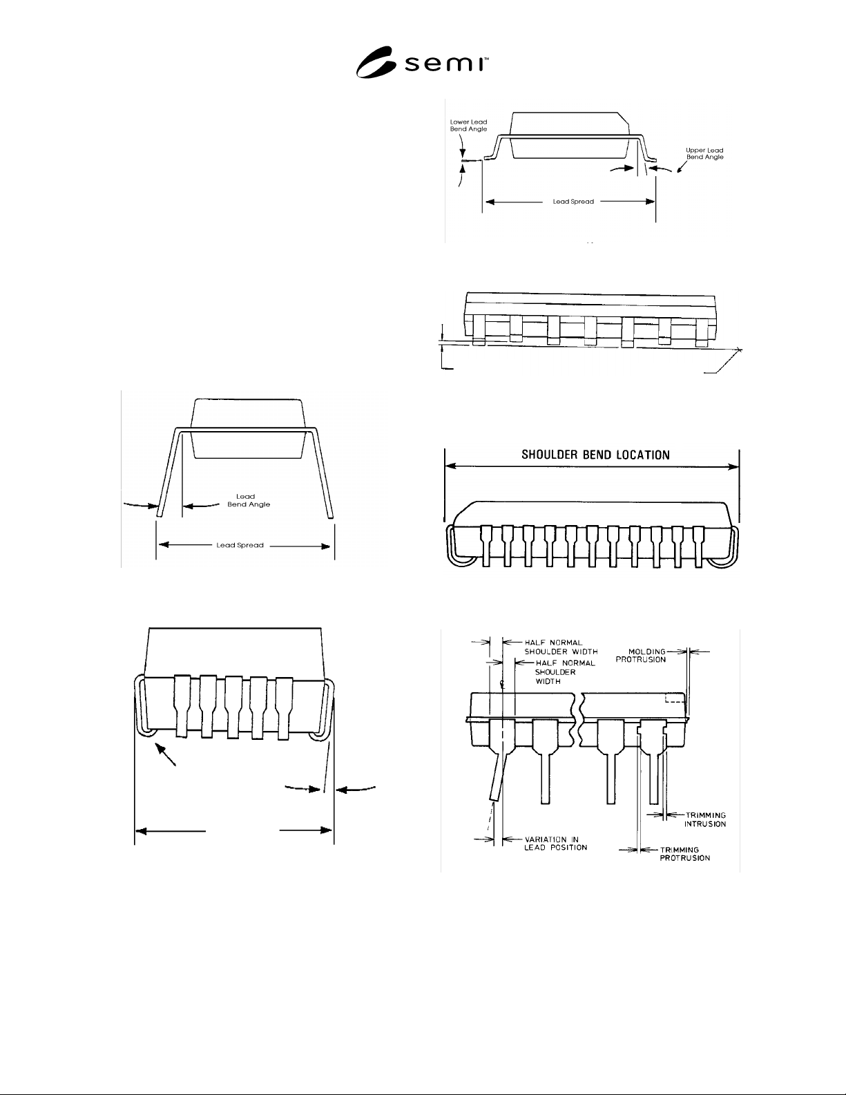
Figure 1A
PDIP Package
Foot
Radius
Lead
Bend Angle
Lead Spread
Figure 1B
PLCC Package
Figure 1C
SOIC and PQFP Packages
Vertical Lead
Position
Reference Plane
Figure 2
Lead Co-planarity
Figure 3
Shoulder Bend Location
Figure 4
Parting Line Protrusion, Lead Sweep and Lead
Shoulder Protrusions and Intrusions
SEMI G54-93 © SEMI 19935
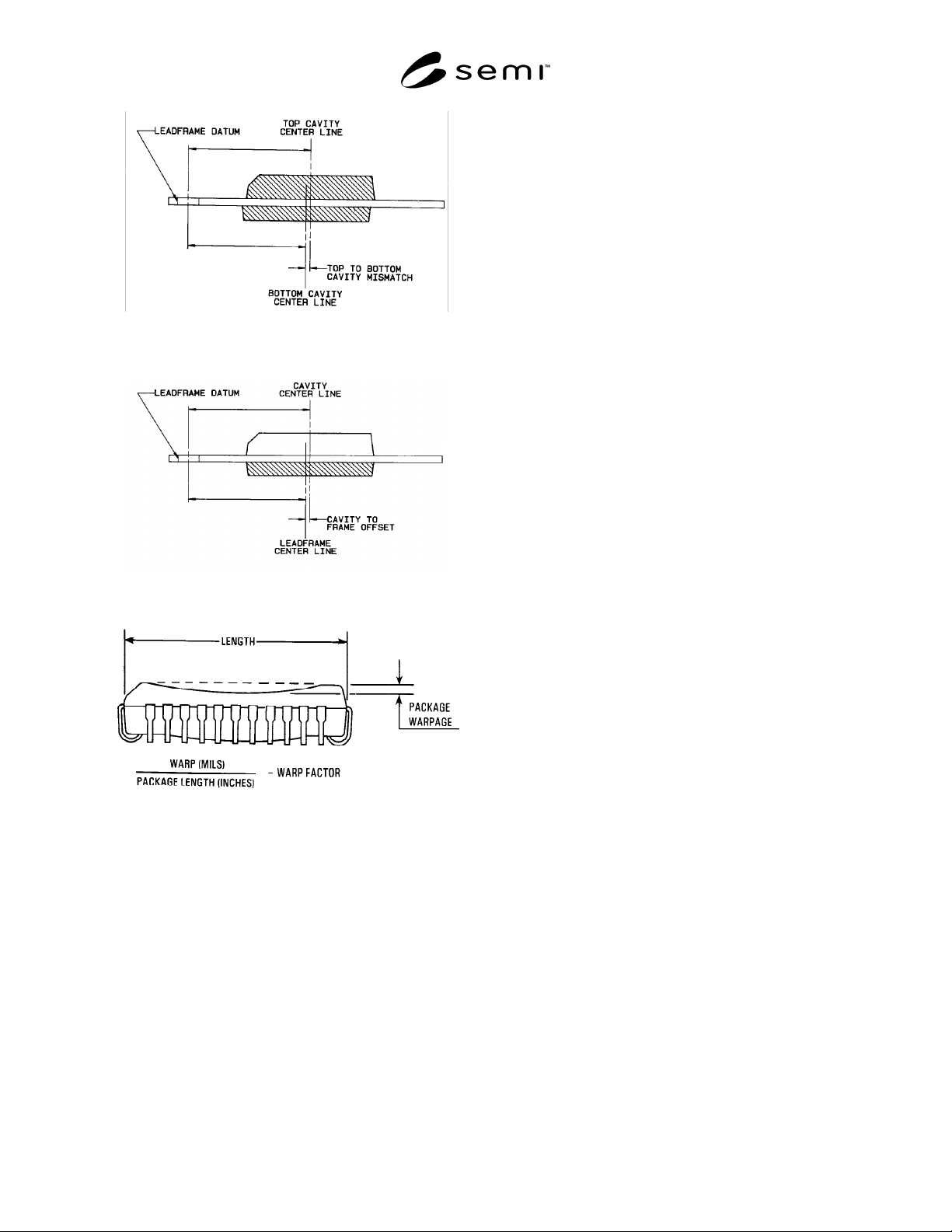
Figure 5
Mismatch
Figure 6
Offset
Figure 7
Package Warpage
NOTICE: These standards do not purport to address
safety issues, if any, associated with their use. It is the
responsibility of the user of these standards to establish
appropriate safety and health practices and determine
the applicability of regulatory limitations prior to use.
SEMI makes no warranties or representations as to the
suitability of the standards set forth herein for any
particular application. The determination of the
suitability of the standard is solely the responsibility of
the user. Users are cautioned to refer to manufacturer’s
instructions, product labels, product data sheets, and
other relevant literature respecting any materials
mentioned herein. These standards are subject to
change without notice.
The user’s attention is called to the possibility that
compliance with this standard may require use of
copyrighted material or of an invention covered by
patent rights. By publication of this standard, SEMI
takes no position respecting the validity of any patent
rights or copyrights asserted in connection with any
item mentioned in this standard. Users of this standard
are expressly advised that determination of any such
patent rights or copyrights, and the risk of infringement
of such rights, are entirely their responsibility.
Copyright by SEMI® (Semiconductor Equipment and Materials
International), 3081 Zanker Road, San Jose, CA 95134. Reproduction o
f
the contents in whole or in part is forbidden without express written
consent of SEMI.