semi合集-English.pdf - 第5133页
SEMI M29-1296 © SEMI 1996, 2003 13 APPENDIX 1 APPLICATION NOTES NOTICE : This ap pendix was approved as a part of SEM I M29 by full lette r ballot proce dure. A1-1 Heat-Resistant Temperature A1-1.1 Parts defined herein a…
SEMI M29-1296 © SEMI 1996, 2003 12
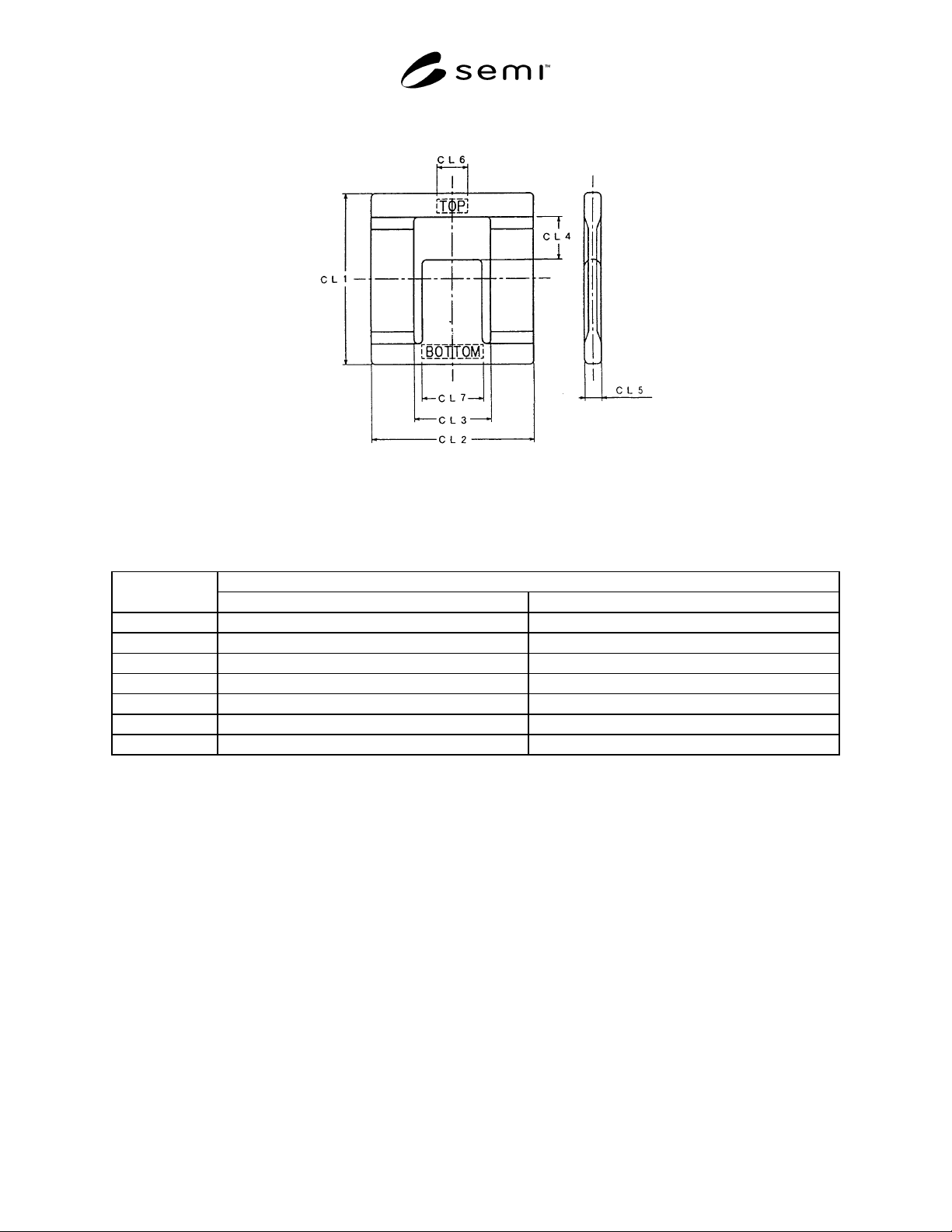
5.6 Clamp — Dimensions of a clamp are shown in Figure 16 and Table 6.
Figure 16
Clamp
Table 6 Dimensions of Clamp
Unit: mm
Standardized Dimension
Location
13 Wafers 25 Wafers
CL1 100 ± 10 ←
CL2 95 ± 2 ←
CL3 45 ± 2 ←
CL4 25 ± 1 ←
CL5 10 max ←
CL6 20 ± 5 ←
CL7 40 ± 10 ←
5.7 Gasket — A gasket is a part to be mainly designed with maker’s know-how regarding its material and form. In
addition, this is frequently revised for increase of quality.
5.7.1 Since there is no practical problem so long as its position is decided, the gasket is not defined. However, it
should be provided in the area defined in Sections 5.3.3 and 5.4.3.
SEMI M29-1296 © SEMI 1996, 2003 13
APPENDIX 1
APPLICATION NOTES
NOTICE: This appendix was approved as a part of SEMI M29 by full letter ballot procedure.
A1-1 Heat-Resistant Temperature
A1-1.1 Parts defined herein are not considered to be used under high temperature because it is assumed to be used
under the usual conditions. As for operating temperature of each part, information from its maker should be
confirmed.
A1-2 Orientation of Wafers in Transportation
A1-2.1 It is necessary to vertically keep wafers in transportation. Therefore, it is necessary to clarify vertical
holding indicated on buffering material and carton boxes.
A1-3 Using Procedure
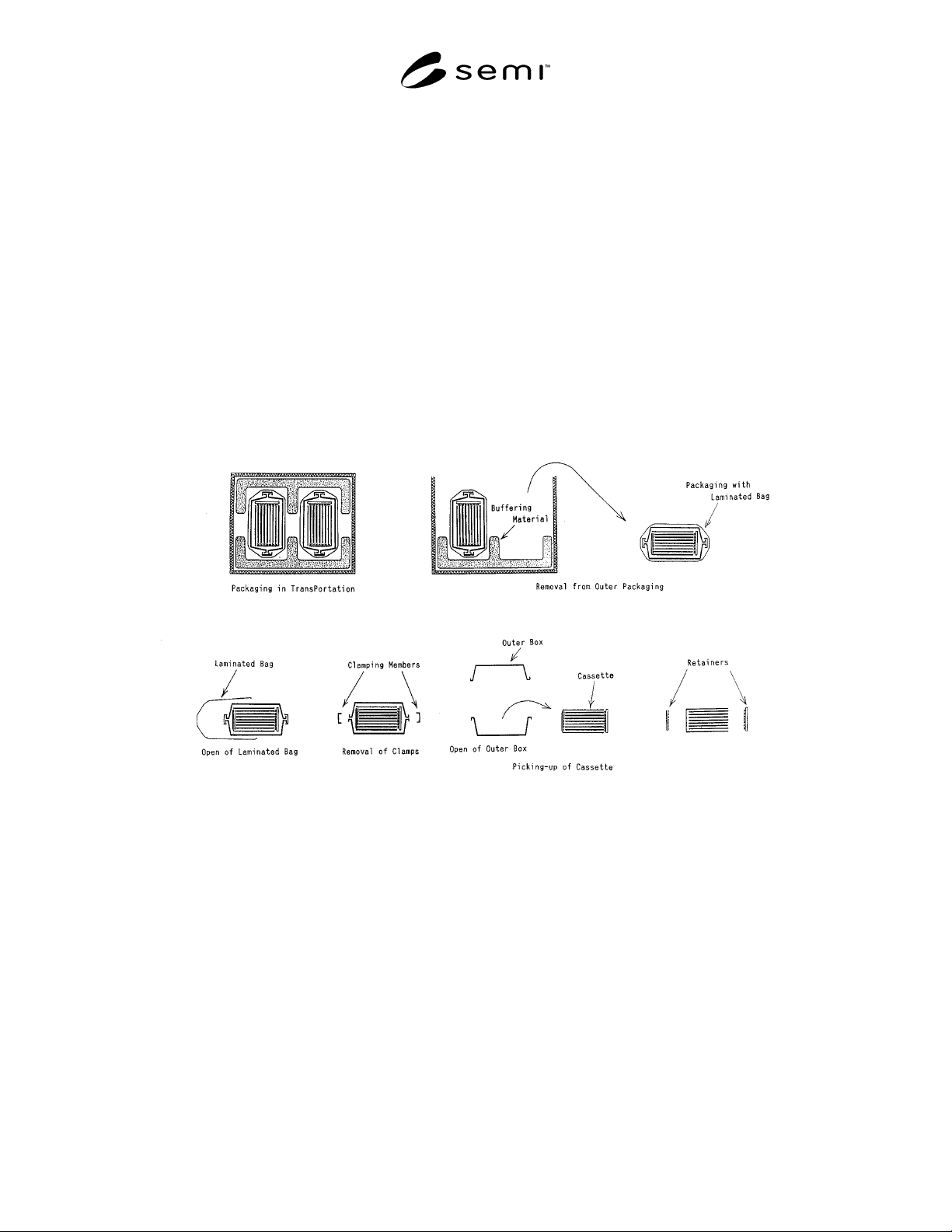
A1-3.1 The procedure for using a shipping box defined in this document is shown in Figure A1-1.
Figure A1-1
Example of Procedure for Using a Shipping Box
A1-4 Maximum Dimensions and Attached Location of Label
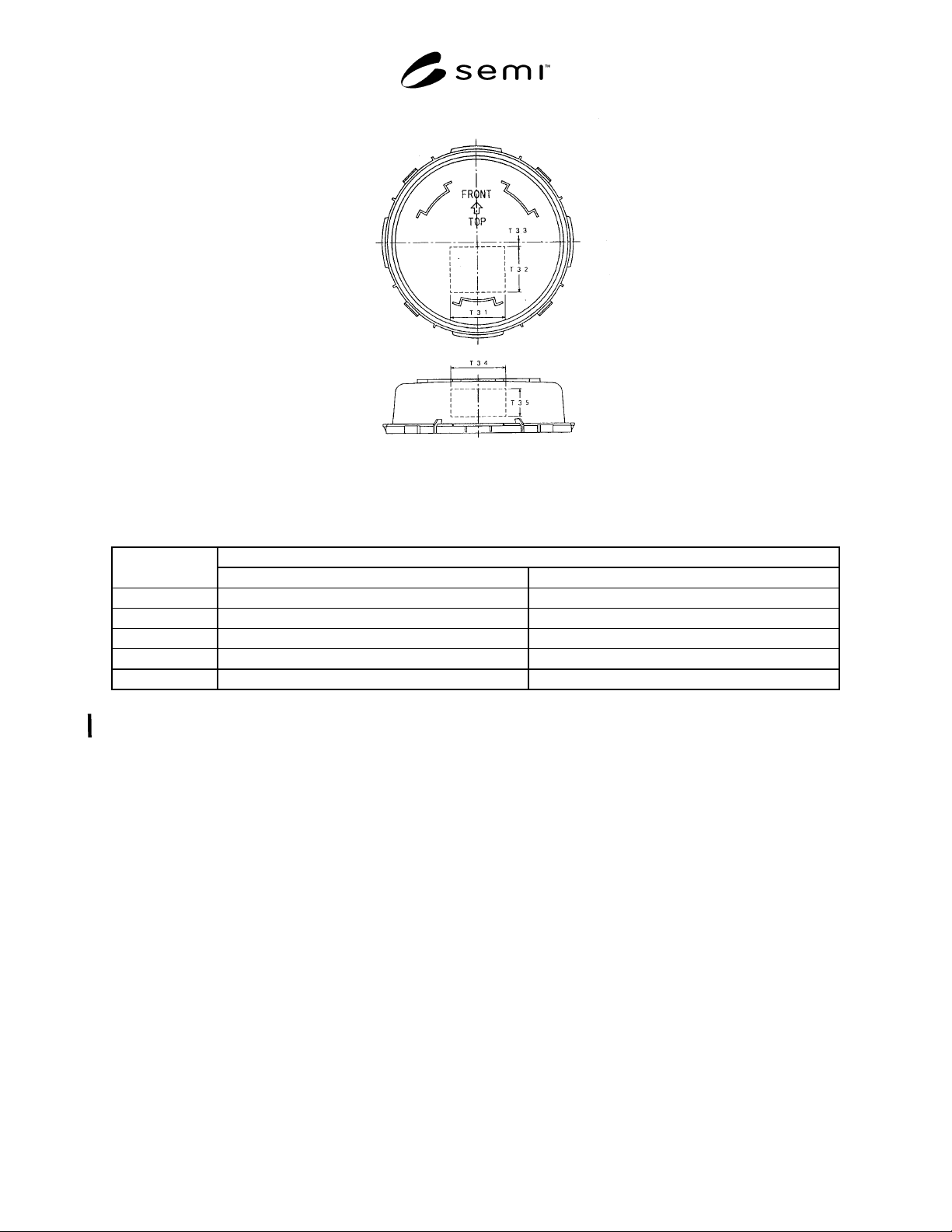
A1-4.1 In case it is necessary to attach a label on a shipping box, the label should be attached in the area shown in
Figure 18 and Table A1-1, and hence, a designer of a shipping box should not provide a projection in this area.
SEMI M29-1296 © SEMI 1996, 2003 14
Figure A1-2
Label Area
Table A1-1 Dimensions of Label Area
Unit: mm
Standardized Dimension
Location
13 Wafers 25 Wafers
T31 120 max ←
T32 100 max ←
T33 10 min ←
T34 120 max ←
T35 60 max ←
NOTICE: SEMI makes no warranties or representations as to the suitability of the standards set forth herein for any
particular application. The determination of the suitability of the standard is solely the responsibility of the user.
Users are cautioned to refer to manufacturer’s instructions, product labels, product data sheets, and other relevant
literature respecting any materials mentioned herein. These standards are subject to change without notice.
The user’s attention is called to the possibility that compliance with this standard may require use of copyrighted
material or of an invention covered by patent rights. By publication of this standard, SEMI takes no position
respecting the validity of any patent rights or copyrights asserted in connection with any item mentioned in this
standard. Users of this standard are expressly advised that determination of any such patent rights or copyrights, and
the risk of infringement of such rights, are entirely their own responsibility.
Copyright by SEMI® (Semiconductor Equipment and Materials
International), 3081 Zanker Road, San Jose, CA 95134. Reproduction o
f
the contents in whole or in part is forbidden without express written
consent of SEMI.