semi合集-English.pdf - 第171页
SEMI E21.1-1296 © SEMI 1992, 2002 3 Figure 2 Proposed 300 mm Interface Plane
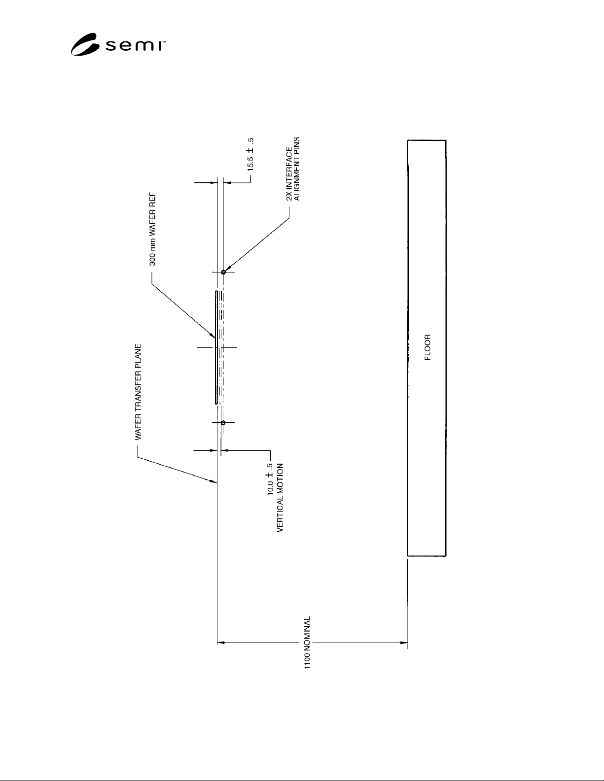
SEMI E21.1-1296 © SEMI 1992, 2002 2
Figure 1
Proposed 300 mm Wafer Transport Plane Elevation
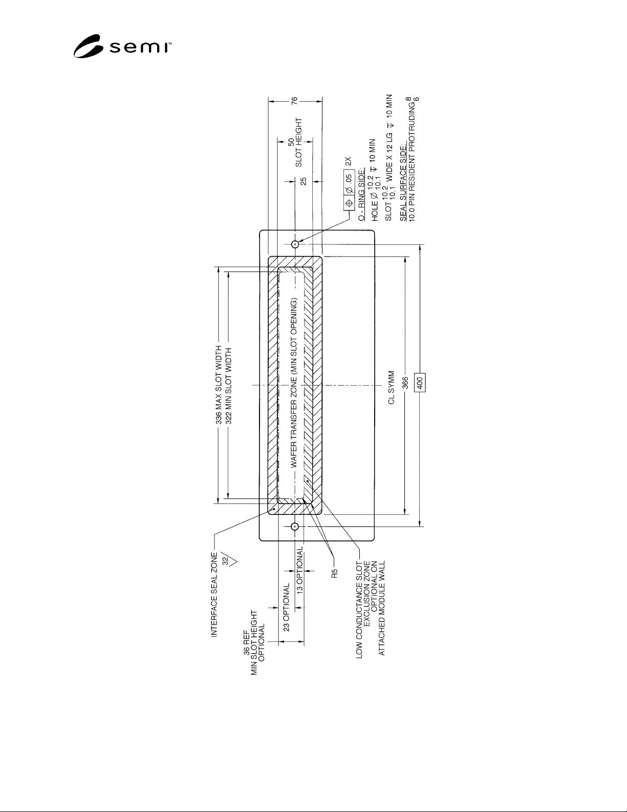
SEMI E21.1-1296 © SEMI 1992, 2002 3
Figure 2
Proposed 300 mm Interface Plane

SEMI E21.1-1296 © SEMI 1992, 2002 4
NOTICE: SEMI makes no warranties or representations as to the suitability of the standards set forth herein for any
particular application. The determination of the suitability of the standard is solely the responsibility of the user.
Users are cautioned to refer to manufacturer' s instructions, product labels, product data sheets, and other relevant
literature, respecting any materials or equipment mentioned herein. These standards are subject to change without
notice.
The user’s attention is called to the possibility that compliance with this standard may require use of an invention
covered by patent rights. By publication of this standard, Semiconductor Equipment and Materials International
(SEMI) takes no position respecting the validity of any patent rights asserted in connection with any item mentioned
in this standard. In particular, users of the specification should be aware that Drytek, Inc., A Unit of General Signal,
16 Jonspin Road, Wilmington, MA 01887-1087, Phone: (508) 657-3933, has neither claimed nor disclaimed that
compliance with this specification would require use of an invention covered by one or more of its patents. Users of
this standard are expressly advised that determination of any such patent rights, and the risk of the infringement of
such rights, are entirely their own responsibility.