semi合集-English.pdf - 第7424页
SEMI MF1529-1104 © SEMI 2004 5 parameter for the proper probe ty pe in a gi ven appli cation. The combination of probe radius and force that is chos en affects both the likelihood of probe pen e tration and the quality o…

SEMI MF1529-1104 © SEMI 2004 4
SEMI MF81 — Test Method for Measuring Radial
Resistivity Variation on Silicon Wafers
SEMI MF84 — Test Method for Measuring Resistivity
of Silicon Wafers with an In-line Four-Point Probe
SEMI MF374 — Test Method for Sheet Resistance of
Silicon Epitaxial, Diffused, Polysilicon, and Ion-
Implanted Layers Using an In-Line Four-Point Probe
with the Single-Configuration Procedure
SEMI MF1241 — Terminology of Silicon Technology
SEMI MF1618 — Practice for Determination of
Uniformity of Thin Films on Silicon Wafers
4.2 ASTM Standard
D 5127 — Guide for Ultra Pure Water Used in the
Electronics and Semiconductor Industry
6
NOTICE: Unless otherwise indicated, all documents
cited shall be the latest published versions.
5 Terminology
5.1 For definitions of terms used in silicon wafer
technology refer to SEMI M1 and SEMI MF1241.
6 Summary of Test Method
6.1 An in-line four-point probe is used to determine the
specimen sheet resistance at each desired measurement
location.
6.1.1 The number and positioning of measurement
locations is determined by end-use needs, or by the
parties to the test in the case of referee measurements.
6.1.2 At each location, a direct current is passed into the
specimen, using two of the probes, as specified, and the
potential difference is measured using the other two
probes.
6.1.3 Current polarity is reversed and the potential
difference is re-measured to allow elimination of
thermoelectric effects.
6.1.4 Before the probe is raised, the process is repeated
using a different combination of probes, as specified.
At each location, the sheet resistance is obtained from
the four ratios of potential difference to current.
6.2 The adequacy of the probe is determined both by
optical examination of probe indentations made in a
polished silicon surface, and by a performance test on a
wafer of the type whose uniformity is to be checked.
6.3 The accuracy of the electronics is tested by means
of an analog circuit emphasizing the performance and
6 Annual Book of ASTM Standards, Vol 11.01, ASTM International,
100 Barr Harbor Drive, West Conshohocken, PA 19428. Telephone:
610-832-9500, Fax: 610-832-9555, Website:
www.astm.org
.
noise immunity of the electronics in the presence of
large contact resistances of the probe tips to the
semiconductor surface.
7 Apparatus
7.1 Specimen Preparation
7.1.1 Chemical Laboratory Apparatus — Such as
plastic beakers, graduated cylinders, and plastic coated
tweezers for use both with acids and with solvents.
Proper facilities for handling and disposing of acids and
their vapors are essential.
7.1.2 Hot Plate — Large enough to heat wafer of
interest to 200°C.
7.2 Probe Assembly
7.2.1 Four-point Probe — Having conical probe tips of
a durable material such as tungsten-carbide. The
included angle of the tips shall be in the nominal range
45 to 150°. The probe tips shall be in a straight line
with nominally equal separations in the range 250 m
(0.010 in.) to 1.59 mm (0.0625 in.). An isolation
resistance between adjacent probes, a factor of 10
5
larger than the sheet resistance of the film is required; a
value of 10
9
, or greater, is recommended for the
widest general application. Recommended tip radii and
probe force values are slightly different depending upon
whether the probe force is applied by springs, or
deadweight, as follows:
7.2.1.1 Spring-loaded Probes — Having tips that
terminate in a radius in the nominal range 25 to 250 m
or in a flat circular truncation of the cone with a circle
diameter in the range 50 to 125 m. A probe force per
pin of 0.25 to 2.0 N (approximately 25 to 200 gf) may
be needed to cover the variety of films that are covered
under the scope of this test method.
7.2.1.2 Deadweight-loaded Probes — Having probe
tips that terminate in a radius of at least 19 m. A
probe force per pin of 0.1 to 1 N (approximately 10 to
100 gf) may be needed to cover the variety of films that
are covered under the scope of this test method.
NOTE 4: In general, the blunter the probe tip, the higher the
probe force that is used to make good electrical contact to the
layer. Conversely, the sharper the probe tip, or the thinner the
layer, the lighter the probe force that should be used. The
upper end of the allowed probe force range is generally used
only for buried-peak conducting layers, such as MeV
implants, or for high-resistivity, thick epitaxial layers.
General experience indicates that there is not a simple
specification of one or two combinations of probe radius and
probe force that will cover all layers of interest. Experience
with conditioning probe tips against materials such as a
sapphire or non-polished ceramic substrate, or even on a piece
of lapped silicon, indicates that the microroughness of the
probe tip is a very important, but not-readily specifiable

SEMI MF1529-1104 © SEMI 2004 5
parameter for the proper probe type in a given application.
The combination of probe radius and force that is chosen
affects both the likelihood of probe penetration and the
quality of electrical contact, which in turn affects the
measurement noise and accuracy. A use test is given to aid in
verifying appropriateness of a given probe for a specific layer
type. Controlled lowering of the probe pins so that contact is
made without lateral scrubbing of the probes against the wafer
surface has been found to be very important.
7.3 Microscope
7.3.1 The microscope for inspecting probe damage shall
have a magnification of at least 600×, and an eyepiece
magnification no greater than 15×. The microscope
shall be capable of dark-field, interference contrast, or
oblique illumination.
7.3.2 The microscope shall have a stage capable of
moving the specimen in order to examine a number of
adjacent damage marks made by each of the four probe
points.
7.4 Measurement Stage
7.4.1 Wafer Prober Stage — With a vacuum chuck or
comparable means of holding the wafer securely during
measurement. This vacuum chuck should be of
sufficient thermal mass to keep the wafer at a constant
temperature, within 1°C, during the time required for
all measurements. The stage should be provided with
stops, pins, engraved circles, or other means for
accurately and repeatedly positioning wafers. For
measurements on wafers where the deposited or
fabricated film may extend over the edges of the
substrate and make contact to the backside, a thin layer
of mica, or other electrical insulator must be used
between the wafer and the chuck.
7.4.2 Probe Assembly Support that allows the probes to
be lowered onto the wafer surface with no evidence of
lateral movement (probe skidding). This requirement
can be verified by lowering and raising the probes a
number of times onto a polished silicon surface with
steps of 50 to 100 m between these locations, and then
observing the probe damage marks for each of the
probe points with the required microscope.
NOTE 5: For a probe with blunt tips or well-conditioned
probe points, it is generally very difficult to view the probe
damage with bright field illumination; use of dark-field,
Nomarski, or oblique illumination is recommended. To aid in
locating the probe damage, the formation of a grid of
rectangles, by scribing, etching or other suitable process on a
polished wafer surface, has been found helpful. The
rectangles should be large enough to allow all four probe
points to be readily located within the boundaries and a
number of probe impressions to be made within the confines
of a single rectangle.
7.4.3 Wafer Probe Stage with a sufficient range of
motion to allow probing all desired locations on the
largest wafers to be measured. Except for restrictions
on the exclusion of three probe spacings at the
perimeter of the layer being measured, the accuracy of
sheet resistance measurements using this test method do
not require any particular accuracy on the position
coordinates.
NOTE 6: If this test method is used for referee
measurements, uncertainty in position coordinates may
produce accurate measurements at the locations measured but
may make comparison of data more difficult. It is
recommended that the wafer be centered on the stage with an
accuracy of 1 mm, or better, and that all positions measured,
have coordinates controlled with an accuracy of 10 m, or
better, with respect to the center of the stage.
7.4.4 The wafer stage shall be instrumented with a
temperature monitor to be used for any application
where the average sheet resistance of the layer is a
parameter to be reported. The temperature monitor
may be of any convenient type, but must be accurate to
0.3°C, or better.
7.5 Electrical Measuring Apparatus
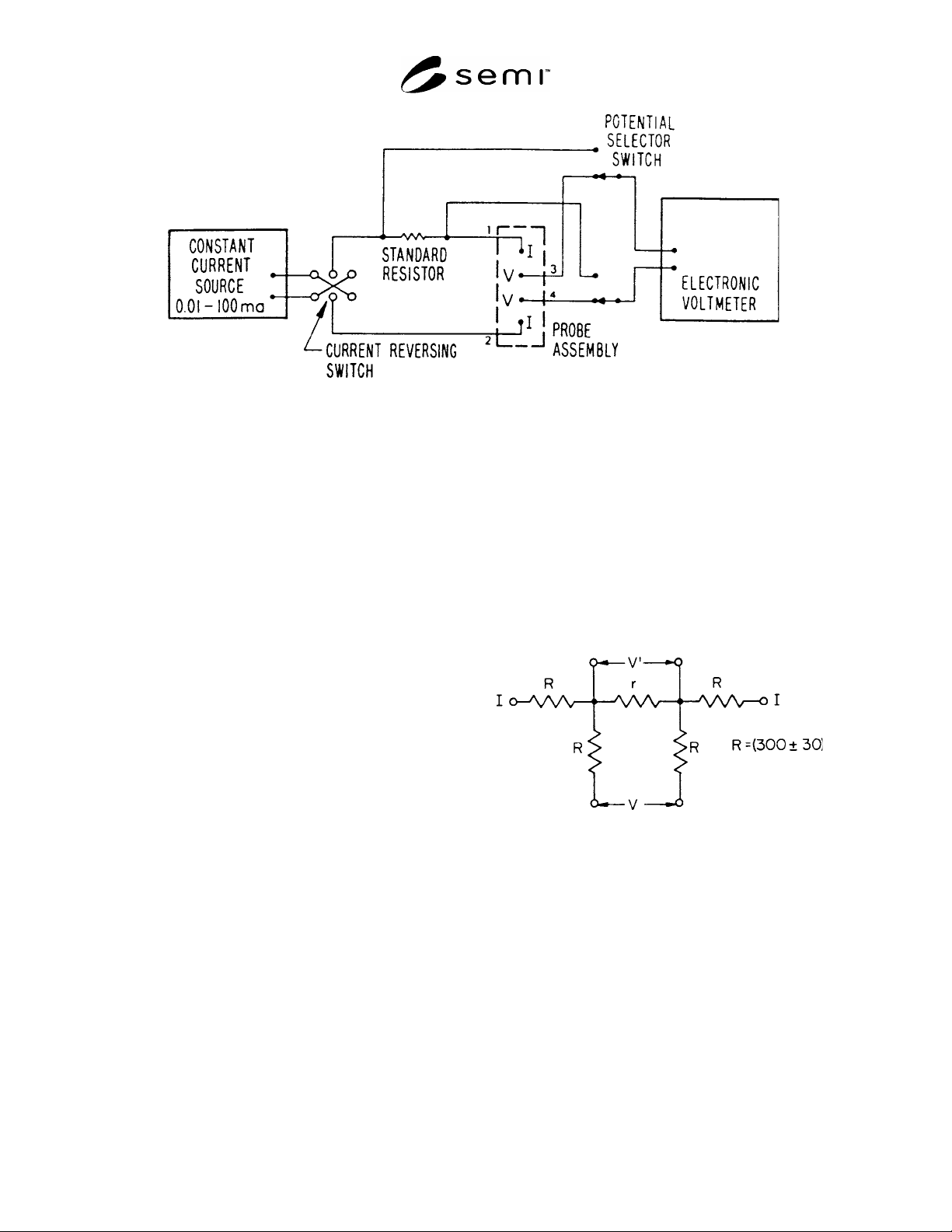
7.5.1 The conceptual layout of the electronic circuitry is
shown in Figure 1 for the case where a standard resistor
is used to monitor the applied current. The standard
resistor can be omitted if the current value is set or
known directly.
7.5.1.1 Constant DC-Current Source — Having
sufficient compliance voltage to supply a constant
current that results in a measured voltage drop on the
specimen that is between 5 and 20 mV. Currents
between 10
6
and 10
2
A are required if the sheet
resistance range 1 to 20,000 is to be covered. The
output current must be stable to 0.01%, or better, during
the time required to take all data at each location; ripple
and other noise must be less than 0.1% of the dc-current
level. A compliance voltage in excess of 10 V is
generally not needed unless measurements must be
made through a significant layer of oxide or other
dielectric. A standard resistor (Section 7.5.1.2) is
needed to determine measurement current unless the
current supply is in calibration and known to output a
dc-current that is within 0.1% or better of the set-point
value. A wet or dry battery may be used for the current
source providing there is means for regulating the
output current.
SEMI MF1529-1104 © SEMI 2004 6
Figure 1
Schematic of Measurement Circuit Showing Use of a Standard Resistor
and a Probe Wired for Configuration A
NOTE 7: to semiconductor effects occurring at higher
measurement currents are avoided. However, for certain
applications of interest, such as metal films and very heavily
doped silicon substrates, it will generally be necessary to
accept measurements with fewer significant figures or else to
use a current supply with an output above the common
maximum of 100 mA, or else to use a voltmeter with sub-
microvolt resolution.
7.5.1.2 Standard Resistor — Used to monitor the value
of the measurement current if the current supply does
not meet the accuracy of settability given in Section
7.5.1.1. The standard resistor shall be selected to give a
potential difference of 0.5 to 5 times that measured
across the specimen. This requires the standard resistor
to have a value from 2.5 to 25 times the sheet resistance
of the layer. The value of the standard resistor must be
known at least to four significant digits.
7.5.1.3 Switches — Double pole, double throw switch
for reversing the direction of the current, and four pole,
double throw switch for changing the probe
configuration. The switching functions may be
accomplished by wafer switches or relays. Isolation
between all switch poles or relays must be 10
6
times the
sheet resistance of the layer being measured; isolation
of 10
9
, or greater is recommended.
7.5.1.4 Electronic Voltmeter — To read the potential
difference across the specimen and standard resistor, or
if calibrated in conjunction with the current source, to
read the voltage-current ratio directly. The voltmeter
shall be capable of measuring dc voltages between 1
and 100 mV full scale, and be able to resolve the
measured voltages to 0.01%, or better. The meter must
have an input impedance of at least 10
9
.
7.5.2 Analog Test Circuit — Five resistors connected as
shown in Figure 2 shall be used according to the
measurement electronics qualification procedure of
Section 11.3 for evaluating the accuracy and precision
of the electronics in the presence of large series
resistors simulating the probe contact resistances.
Several circuits of this type may be needed with the
resistance of the central resistor, r, of each being,
selected according to the expected sheet resistance of
the layer to be measured, as listed in Table 2.
Figure 2
Analog Test Circuit, Simulating the Contact
Resistances in a Four-Probe Measurement
7.5.3 Conductivity-Type Instrument — Apparatus in
accordance with Method A of SEMI MF42.
7.6 Computer Control — It is intended that this test
method will be under control of a computer for
positioning the sample at each of the intended
measurement sites, lowering the probes, and performing
all necessary control of circuit switching, setting of
current values, and measuring and logging voltages. It
is beyond the scope of this test method to specify
details of the computer-based automation.