semi合集-English.pdf - 第4976页
SEMI M11-0704 © SEMI 1988, 2004 33 ITEM (See Note 1) p/p − EPITAXIAL WAFER p/p + EPITAXIAL WAFER p/p ++ EPITAXIAL WAFER 12.4b Global Flatness (GFLR or TIR) ≤ 3 µm 12.5 Flatness/Site (See Note 10) SFQR ≤ 90 nm Site Size 2…
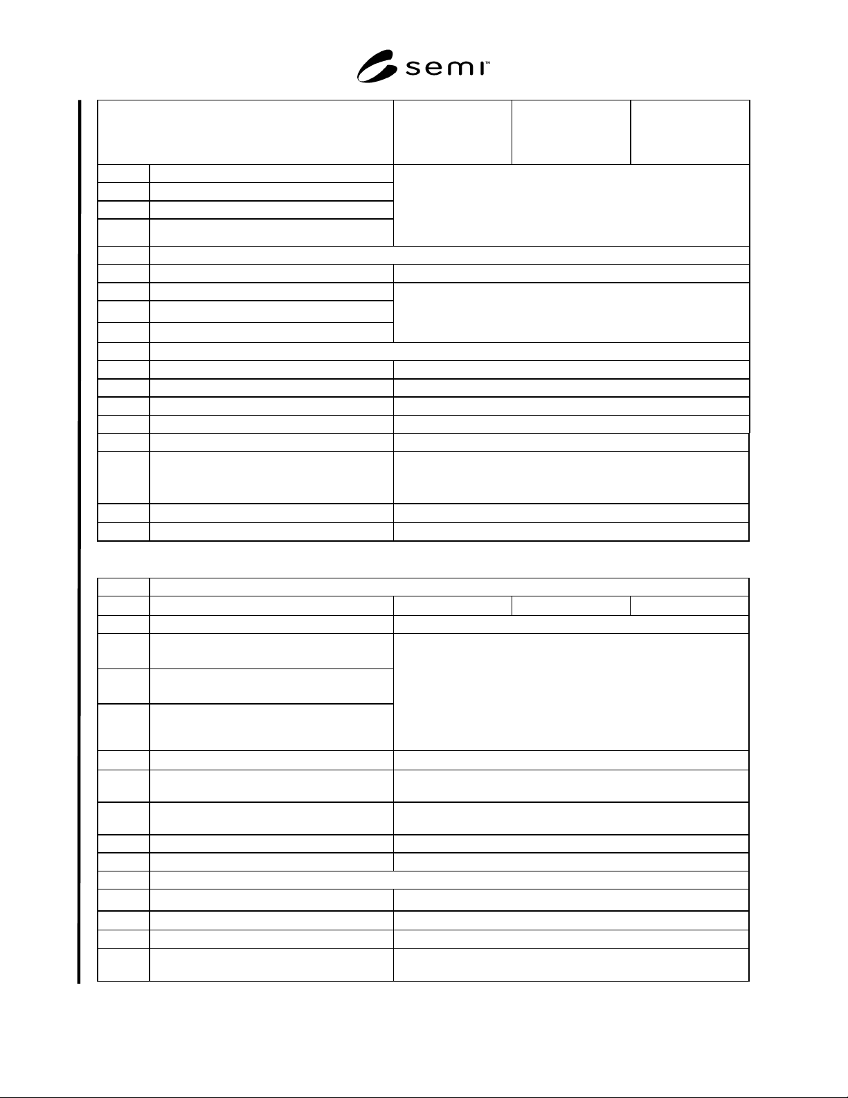
SEMI M11-0704 © SEMI 1988, 2004 32
ITEM (See Note 1)
p/p
−
EPITAXIAL
WAFER
p/p
+
EPITAXIAL
WAFER
p/p
++
EPITAXIAL
WAFER
4.4 Twin
4.5 Swirl
4.6 Shallow pits
4.7 Oxidation-Induced Stacking Faults (OSF)
5.0
WAFER PREPARATION CHARACTERISTICS
5.1 Wafer ID Marking per SEMI M1
5.4 Extrinsic Gettering Treatment
5.5 Backseal
5.6 Annealing
supplier-purchaser agreement
6.0 SUBSTRATE MECHANICAL CHARACTERISTICS (Per SEMI M1 Unless Otherwise Specified)
6.1 Diameter 300 or 200
6.2 Notch Dimensions per SEMI M1
6.3 Notch Orientation <110> ± 1°
6.61 Edge Profile per SEMI M1
6.6.2 Edge Surface Finish Polished
6.7 Substrate Thickness
775 ± 20 µm [300 mm diameter]
or
725 ± 20 µm [200 mm diameter]
6.8 Thickness Variation (GBIR)
≤ 3 µm
6.9 Surface Orientation and Tolerance (100) ± (0.2 – 1)°
EPITAXIAL WAFER
(Epitaxial Layer and Substrate)
11.0
EPITAXIAL LAYER CHARACTERISTICS
11.1 Conductivity Type
p/p
−
p/p
+
p/p
++
11.2 Primary Dopant Boron
11.3 Silicon Source Gas
11.4 Epi Growth Method
11.5
Carrier Density Range - Must be met at all
points on the wafer surface inside the edge
exclusion (See Note 13)
supplier-purchaser agreement
11.6 Net Carrier Density Variation
≤ 15%
11.7
Layer Thickness (Target Value at Wafer
Center and Tolerance)
Target: supplier-purchaser agreement
11.8
Thickness Variation (within wafer, per SEMI
M11, Section 6.3)
≤ 10%
11.9 Flat Zone supplier-purchaser agreement
11.10 Transition Width supplier-purchaser agreement
12.0
MECHANICAL CHARACTERISTICS
12.1 Bow supplier-purchaser agreement
12.2 Warp
≤ 50 µm (See Note 3)
12.3 Sori supplier-purchaser agreement
12.4a Total Thickness Variation (GBIR or TTV, see
NOTE 9.)
≤ 4 µm
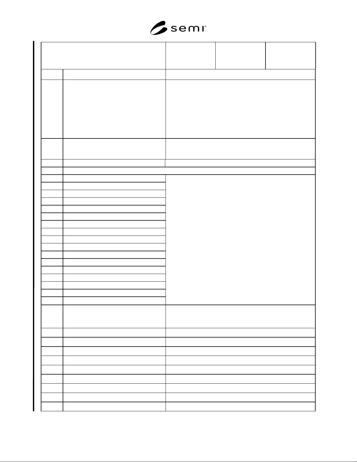
SEMI M11-0704 © SEMI 1988, 2004 33
ITEM (See Note 1)
p/p
−
EPITAXIAL
WAFER
p/p
+
EPITAXIAL
WAFER
p/p
++
EPITAXIAL
WAFER
12.4b
Global Flatness (GFLR or TIR)
≤ 3 µm
12.5 Flatness/Site (See Note 10)
SFQR ≤ 90 nm
Site Size 26 mm x 8 mm
Percent Usable Area ≥ 95%
Partial Sites Included
Or
Percent Usable Area 100%
Full Sites Only
X-offset = 0 and Y-offset = 0
12.7
Nanotopography for each analysis area at a
specified percentage defective
(See SEMI M43)
supplier-purchaser agreement
12.8 Misfit Dislocations supplier-purchaser agreement
13.0
FRONT SURFACE CHARACTERISTICS
13.2 Slip (Note 15)
TBD Dislocation Density
TBD Contamination/Area
TBD Edge Cracks
13.5a Scratches – macro
13.5b Scratches – micro
13.6 Dimples
13.7 Orange Peel
13.8 Cracks/Fractures
13.9 Crow’s Feet
13.10 Edge Chips
13.11 Edge Crown
13.12 Haze
13.13 Foreign Matter
TBD Saw Marks
TBD Dopant Striation Rings
TBD Stains
none
13.14
Localized Light Scatters (LLS)
(300 mm diameter, scale for 200 mm)
Size ≥ 90 nm Count ≤ 238 (Note 11, 16, 17)
Size ≥ 300 nm Count ≤10 (Note 17)
Size ≥ 2,000 nm Count ≤ 5 (See Note 14)
TDB
Surface Metal Contamination (See Note 3)
TDB Sodium
≤ 1 × 10
10
/cm
2
TDB Aluminum
≤ 1 × 10
10
/cm
2
TDB Potassium
≤ 1 × 10
10
/cm
2
TDB Chromium
≤ 1 × 10
10
/cm
2
TDB Iron
≤ 1 × 10
10
/cm
2
TDB Nickel
≤ 1 × 10
10
/cm
2
TDB Copper
≤ 1 × 10
10
/cm
2
TDB Zinc
≤ 1 × 10
10
/cm
2
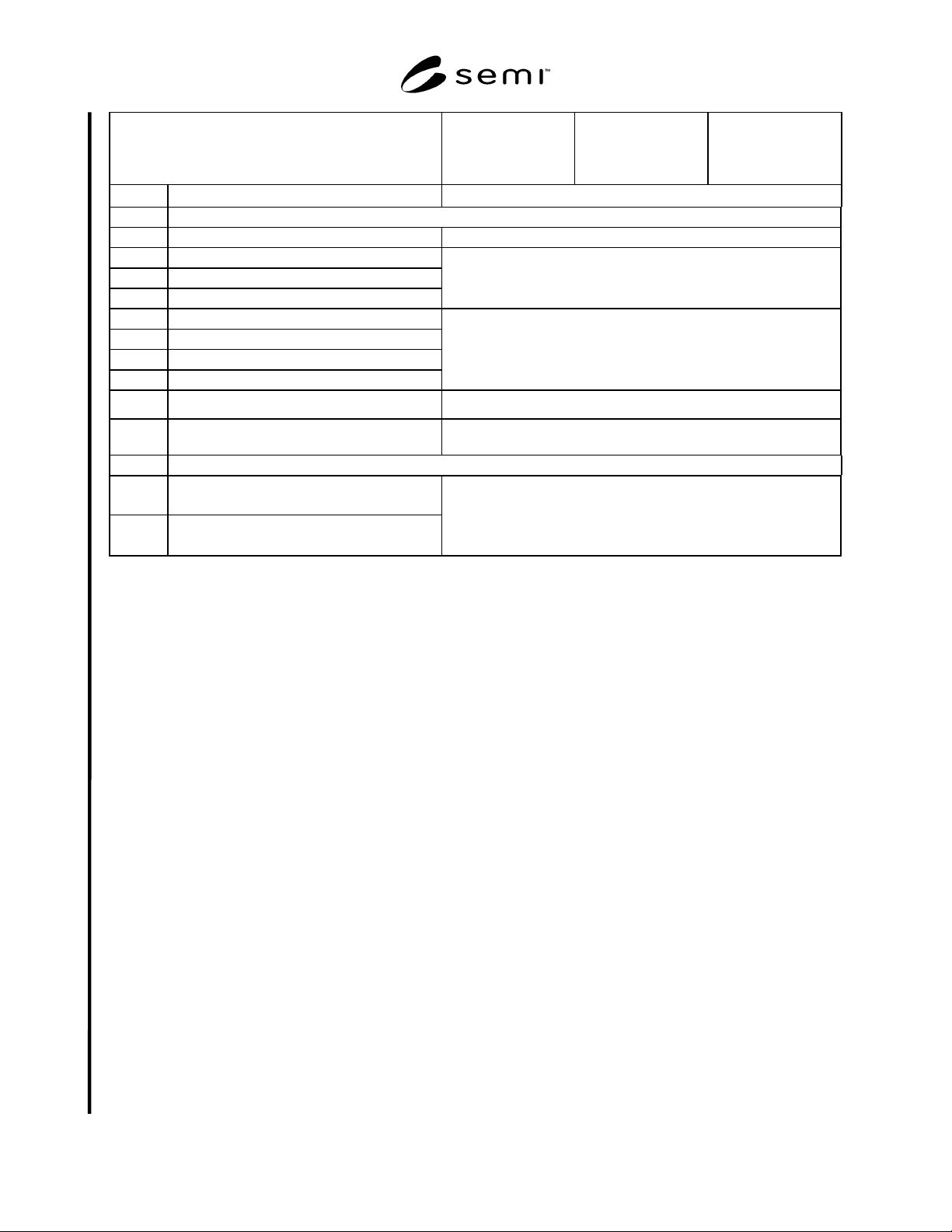
SEMI M11-0704 © SEMI 1988, 2004 34
ITEM (See Note 1)
p/p
−
EPITAXIAL
WAFER
p/p
+
EPITAXIAL
WAFER
p/p
++
EPITAXIAL
WAFER
TDB Calcium
≤ 1 × 10
10
/cm
2
14.0
BACK SURFACE CRITERIA
14.1 Contamination/Area none
14.2 Scratches – macro
14.3 Scratches – micro
14.4 Localized Light Scatterers
supplier-purchaser agreement
TBD Edge Chips
TBD Cracks, Crow's Feet
TBD Saw Marks
TBD Stains
none
TBD Roughness Polished
TBD
Brightness (Gloss) 60° angle of incidence,
referenced to a mirror polished wafer.
≥ 80% (See Note 12)
15.0
OTHER CHARACTERISTICS
TBD
Denuded Zone
Free of Bulk Micro-defects (BMD)
TBD
BMD(Bulk Micro-defect Density)
Thermal Cycle per SEMI MF1239)
supplier-purchaser agreement
NOTE 1: The first column under item references SEMI Standard M18. M18 was in the process of substantial revision at the time this
documented was balloted. Many M18 line references remain to be determined. TBD is the abbreviation for “to be determined”.
NOTE 2: Unless otherwise agreed upon for a specific characteristic or test method.
NOTE 3: Only process control data is required. Data not required on Certificate of Compliance. A larger warp value may be appropriate if a
oxide layer is deposited on the back of the substrate.
NOTE 4: Oxygen level in itself should not be specified but rather is only a control parameter that may give an indication of the amount of
precipitation that will occur after some thermal process that nucleates and grows Bulk Micro-defects generated at precipitates. Addition of
nitrogen or carbon (above the background level) to the crystal can enhance the growth of these precipitates.
NOTE 5: Test in accordance with SEMI MF1188, JEIDA 61, or DIN 50438/1. Also see SEMI M44.
NOTE 6: Test in accordance with SEMI MF1366 or Gas Fusion Analysis, as agreed between supplier and purchaser. Non-destructive metrology
did not exist at the time this document was approved.
NOTE 7: Test in accordance with SEMI MF951, Plan A1, A2, or A3, as agreed between supplier and purchaser.
NOTE 8: Non-destructive metrology did not exist at the time this document was approved.
NOTE 9: The 9-point TTV parameter has been replaced by GBIR. See 12.4a.
NOTE 10: SFQR with a site size of 26 mm × 8 mm is approximately equal to SFSR with a site size of 26 mm x 32 mm at the 90 nm technology
level. The smaller site allows more coverage of the FQA than the larger site. The value of site flatness of 90 nm is taken from the ITRS Starting
Materials Table.
NOTE 11: The 90 nm count, 238, may be transformed to another maximum LLS count using draft international standard: ISO/DIS 14644-1
which uses the equation: count per wafer at 65 nm (new minimum size)
= (count per wafer at 90 nm)
*(90 nm / 65 nm)
2.
. For example
converting from a 90 nm minimum size to a 65 nm minimum size yields a count of 456.
NOTE 12: This specification implies a polished back surface.
NOTE 13: The intent in specifying carrier density using a range, rather than the center nominal with tolerance accompanied by a wafer variation
limit, is to minimize the importance of edge variations and to emphasize meeting the range of carrier density as it is allowed by the process and
the designers.
NOTE 14: Large Area Defects (LADs) are surface imperfections or particles that have geometry with at least one side or diameter that is equal to
or greater than the layer thickness. Their actual size cannot be currently implied from the output of an SSIS.
NOTE 15: Slip tested in accordance with SEMI MF1726; an etch depth < 100 nm is acceptable. The metrology used for slip determination is a
major factor in determining the presence or absence of slip lines. X-ray Topography is much more sensitive than the ASTM etching and
microscopic inspection method given here but no Standard Test Method currently exists. X-ray Topography will detect slip that may not
penetrate to the near surface region where the device is fabricated. Use of SSIS equipment set at less ≤90 nm can also reveal slip lines on epi
wafers but again no Standard Test Method currently exists. Surface roughness may interfere with SSIS measurements. With the thermal cycles
employed in 90 nm technology thermal processes, slip propagation should not be a problem.
NOTE 16: Value from the 2003 ITRS 90 nm node.
NOTE 17: May include stacking faults of different scattering intensities and other structural epitaxial defects which are not correctly sized by
current generation SSISs.