semi合集-English.pdf - 第7219页
SEMI MF43-0705 © SEMI 2003, 2005 2 3.1.1 Photoconduct ive and ph otovoltai c effects ca n seriously influ ence the observed resistivity, particularly with nearly intrinsic material. Therefore make all de terminati ons in…

SEMI MF43-0705 © SEMI 2003, 2005 1
SEMI MF43-0705
TEST METHODS FOR RESISTIVITY OF SEMICONDUCTOR
MATERIALS
This test method was technically approved by the global Silicon Wafer Committee. This edition was
approved for publication by the global Audits and Reviews Subcommittee on April 7, 2005. It was available
at www.semi.org in June 2005 and on CD-ROM in July 2005. Original edition published by ASTM
International as ASTM F 43-64T. Last previous edition SEMI MF43-99.
1 Purpose
1.1 The resistivity of a semiconductor material is an important materials acceptance requirement. Resistivity
determinations made during device fabrication are also widely used for quality control purposes.
1.2 These test methods cover two procedures which are widely used for making routine measurements.
2 Scope
2.1 The two test methods in this standard are as follows:
2.1.1 Method A, Two-Probe — This test method requires a bar specimen of measurable cross section and with
cross-sectional dimensions small in comparison with the length of the bar. For materials for which no specific
referee method has been developed, this test method is recommended for materials acceptance purposes.
2.1.2 Method B, Four-Probe — This test method is rapid and does not require a specimen of regular cross section.
This test method may be used on irregularly shaped specimens, provided a flat region is available for the contacting
probes. As described in this standard, this test method is applicable only to specimens such that the thickness of the
specimen and the distance from any probe point to the nearest edge are both at least four times the probe spacing.
For the special case of specimens of circular cross section with thickness more than one, but less than four, times the
probe spacing, measurements by this test method are possible; the required application of approximate geometric
corrections results in improved accuracy (see ¶10.1.3).
2.2 In general, resistivity measurements are most reliable when made on single crystals, since with such material
local variations in impurity which affect the resistivity are less severe. Localized impurity segregation at grain
boundaries in polycrystalline material may result in large resistivity variations. Such effects are common to either of
the measurement test methods but are more severe with the four-probe test method, and its use, therefore, is not
recommended for polycrystalline material.
2.3 The values stated in SI units are to be regarded as the standard. The values given in parentheses are for
information only.
NOTE 1: DIN 50430 is an equivalent method to Method A and DIN 50431 is an equivalent method to Method B.
NOTE 2: Other standardized test methods are preferred for use in various special circumstances. For measurements on thin
wafers, use SEMI MF84; this method is preferred for referee measurements on silicon wafers. For measurements on specimens
for which point contacts are unsatisfactory, use a procedure in ASTM Test Methods F 76 based either on Van Der Pauw or bridge
specimens. For two-probe referee measurements on cylindrical single crystal bars, use SEMI MF397. For four-probe referee
measurements of sheet resistance on epitaxial layers deposited on or diffused or implanted into opposite conductivity-type
substrates, use SEMI MF374.
NOTICE: This standard does not purport to address safety issues, if any, associated with its use. It is the
responsibility of the user of this standard to establish appropriate safety and health guides and determine the
applicability of regulatory or other limitations prior to use.
3 Limitations
3.1 In making resistivity measurements, spurious results can arise from a number of sources. The following must
be guarded against:

SEMI MF43-0705 © SEMI 2003, 2005 2
3.1.1 Photoconductive and photovoltaic effects can seriously influence the observed resistivity, particularly with
nearly intrinsic material. Therefore make all determinations in a dark chamber unless experience has shown that the
material is insensitive to ambient illumination.
3.1.2 Spurious currents can be introduced in the testing circuit when the equipment is located near high-frequency
generators. If equipment is located near such sources, adequate shielding must be provided.
3.1.3 Minority carrier injection during the measurement can occur due to the electric field in the specimen. With
material possessing high minority carrier lifetime and high resistivity, such injection can result in a lowering of the
resistivity for distance of several centimeters. Carrier injection can be detected by repeating the measurements at
lower current. In the absence of injection no increase in resistivity should be observed. It is recommended that the
current used in a resistivity measurement be as low as possible, consistent with the required precision.
3.1.4 Semiconductors have a significant temperature coefficient of resistivity. Consequently, the temperature of
the specimen should be known at the time of the measurement and the current used should be small to avoid
resistive heating. If resistive heating is suspected, it can be detected by a change in readings as a function of time
starting immediately after the current is applied. Temperature coefficients for extrinsic germanium and silicon near
room temperature are available in the literature.
1
For referee purposes, it is recommended that the test be performed
at 23 ± 0.5°C.
NOTE 3: Temperature correction factors for silicon are given in tabular form in SEMI MF84 together with equations for
generating the factors.
3.1.5 Vibration of the probes sometimes causes troublesome changes in the contact resistance. If difficulty is
encountered, shock mount the apparatus.
4 Referenced Standards and Documents
4.1 SEMI Standards
SEMI M1 — Specifications for Polished Monocrystalline Silicon Wafers
SEMI M59 — Terminology for Silicon Technology
SEMI MF84 — Test Method for Measuring Resistivity of Silicon Wafers with an In-line Four-point Probe
SEMI MF374 — Test Method for Sheet Resistance of Silicon Epitaxial, Diffused, Polysilicon, and Ion-implanted
Layers Using an In-line Four-point Probe
SEMI MF397 — Test Method for Resistivity of Silicon Bars Using a Two-point Probe
SEMI MF533 — Test Method for Thickness and Thickness Variation of Silicon Slices
SEMI MF2074 — Guide for Measuring Diameter of Silicon and Other Semiconductor Wafers
4.2 ANSI Standard
B74.10 — Specification for Grading of Abrasive Microgrits
2
4.3 ASTM Standard
F 76 — Test Methods for Measuring Resistivity and Hall Coefficient and Determining Hall Mobility in Single-
Crystal Semiconductors
3
1 Bullis, W. M., Brewer, F. H., Kolstad, C. D., and Swaratzendruber, L. I., “Temperature Coefficient of Resistivity of Silicon and Germanium
near Room Temperature,” Solid State Electron. 11, 639646 (1968).
2 American National Standards Institute, American National Standards Institute, New York Office: 25 West 43rd Street, New York, NY 10036,
USA. Telephone: 212.642.4900, Fax: 212.398.0023, Website:
www.ansi.org
.
3 Annual Book of ASTM Standards, Vol 10.04, ASTM International, 100 Barr Harbor Drive, West Conshohocken, PA 19428. Telephone: 610-
832-9500, Fax: 610-832-9555, Website:
www.astm.org
.
SEMI MF43-0705 © SEMI 2003, 2005 3
4.4 DIN Standards
50430 — Measurement of the Specific Electrical Resistivity of Silicon or Germanium Single Crystals in Bars Using
the Two-probe Direct Current Method
4
50431 — Measurement of the Electrical Resistivity of Silicon or Germanium Single Crystals by Means of the Four-
point-probe Direct Current Method with Collinear Four-probe Array
4
NOTICE: Unless otherwise indicated, all documents cited shall be the latest published versions.
5 Terminology
5.1 Definitions
5.1.1 Terms relating to silicon and other semiconductor technology are defined in SEMI M59.
6 Summary of Test Methods
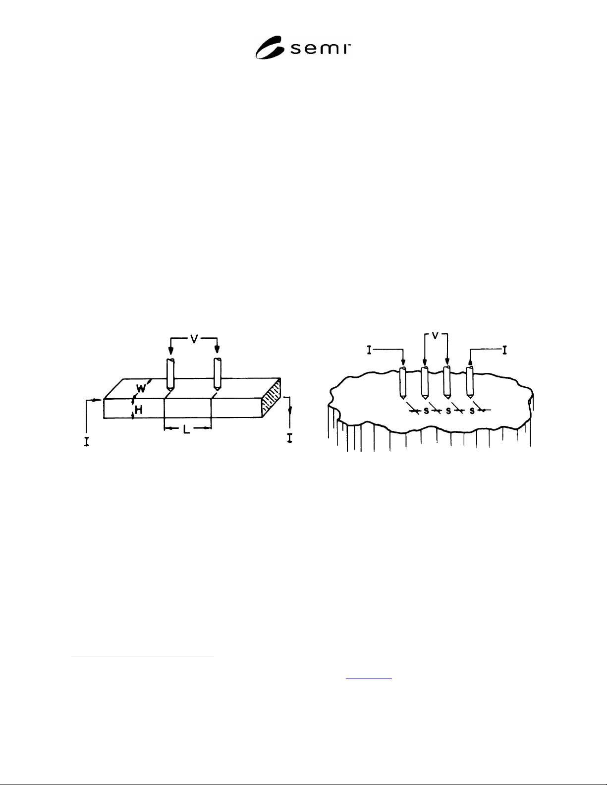
6.1 Two-Probe Method — A direct current, I, is passed through ohmic contacts at the ends of a bar specimen and
the potential difference, V, is determined between two probes placed along the current direction (Figure 1). The
resistivity,
, is calculated from the current and potential values and factors appropriate to the geometry.
6.2 Four-Probe Method — An in-line four-point probe is placed on a flat surface of a solid specimen which can be
approximated as semi-infinite. A direct current, I, is passed through the specimen between the outer probes and the
resulting potential difference, V, is measured between the inner probes (Figure 2). The resistivity,
, is calculated
from the current and potential values and factors appropriate to the geometry.
4 Deutches Institut für Normung e.V., standards are available in both English and German editions from Beuth Verlag GmbH, Burggrafenstrasse
6, 10787 Berlin, Germany, Telephone: 49.30.2601-0, Fax: 49.30.2601.1263, Website:
www.beuth.de.
Figure 1
Specimen and Probe Arrangement for Two-Probe
Measurements on a Rectangular Bar
Figure 2
Specimen and Probe Arrangement for Four-Probe
Measurements on a Semi-Infinite Solid Specimen
7 Apparatus
7.1 Jigs — Suitable for mounting the specimens and contacting them with either two or four probes as required.
7.1.1 Probes — Shall be individually spring mounted and shall be loaded with a force of 1.5 ± 0.5 N. The probes
may be made from hardened tool steel, tungsten carbide, or other conducting metal and may be chisel shaped for
measurement of curved surfaces or pointed for measurement on flat sections. In the case of point probes, the
nominal radius of the tips shall be initially 25 to 50 m. With all probing devices, frequent checking of the probe
spacing with a calibrating microscope is desirable. Probes shall be replaced or resharpened when necessary to
maintain the required spacing tolerance. Isolation resistance between the probes shall be at least 10
9
.