semi合集-English.pdf - 第6480页
SEMI G78-0699 © SE MI 1999 13 Title Description Values mi crons X-direction mils mi crons DUT spacing Y-direction mils mi crons Z clearance mils mi crons Overdrive mils Tes ter-Prober comm unications m ethod OCR on? (Y/N…
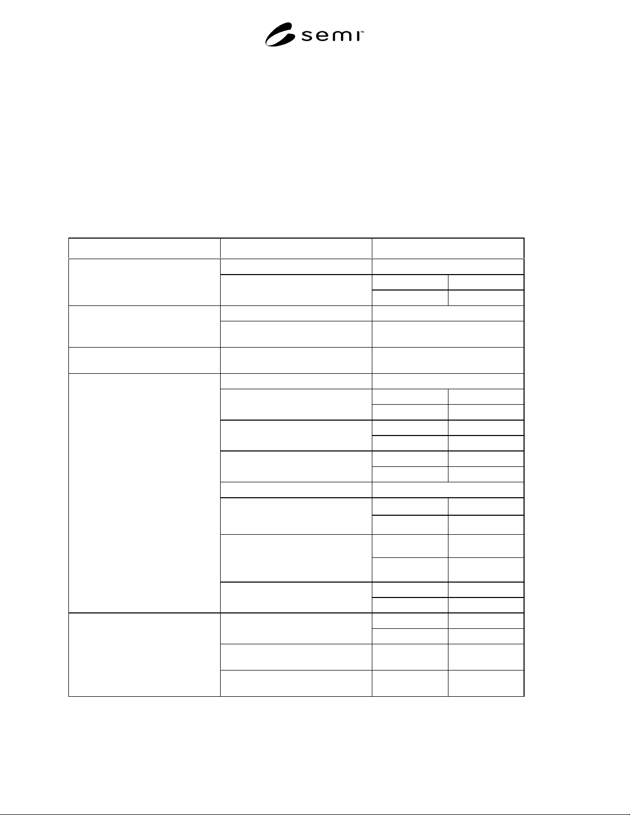
SEMI G78-0699 © SEMI 1999 12
Suggested Graphs for X-Offset and Y-Offset (see Appendix 1 for examples):
X-Offset Y-Offset
LOTX + D-D-X LOTY + D-D-Y
LOTX LOTY
LOTX - D-D-X LOTY - D-D-Y
Average Die X-Offset (3) Average Die Y-Offset (3)
12 Data Collection Table
12.1 The following data are to be recorded about the test environment:
Title Description Values
Installed (Yes/No)
kg
Tester - Prober Interface
If installed, Total Pogo
®
pin force (nominal, calculated)
pounds
Present [docked] (Yes/No)Tester
If present, state manufacturer and
model
Wafer Nominal Die Size (Small, Medium
or Large)
Needle count
gramsNominal force per needle
ounces
micronsDiameter of needle tip
mils
micronsNeedle pitch (within a single row or
column)
mils
Number of needle tiers
mm
Size of needle array in the X
direction (left-to-right when facing
prober (from the operator position))
inches
mmSize of needle array in the Y
direction (away and towards the
operator relative to the center of the
probe card)
inches
mm
Probe Card
Diameter of probe card
inches
ºCSet point / Temperature of chuck
during test
ºF
Soak time, probe card (if test
temperature is other than ambient)
minutes
Test Temperature
Soak time, prober (if other than
ambient)
minutes
SEMI G78-0699 © SEMI 199913
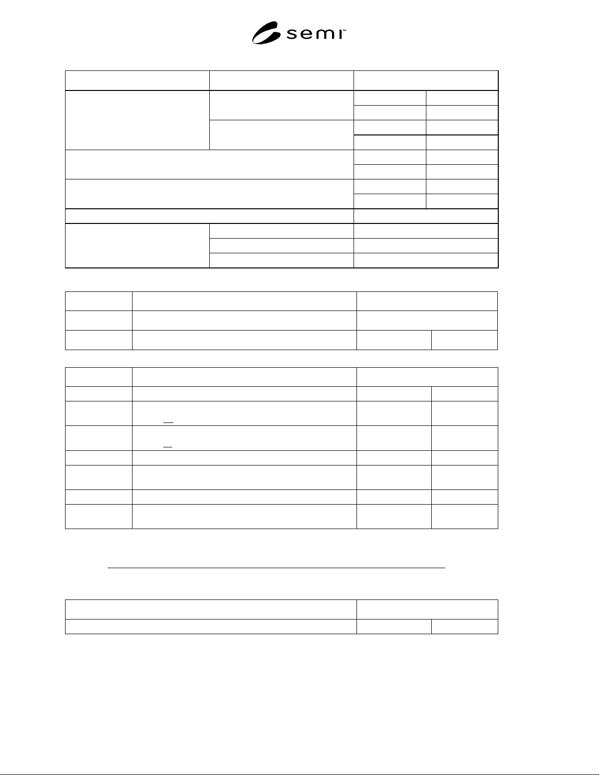
Title Description Values
microns
X-direction
mils
microns
DUT spacing
Y-direction
mils
micronsZ clearance
mils
micronsOverdrive
mils
Tester-Prober communications method
OCR on? (Y/N)
SEMI standard font? (Y/N)
OCR Variables
# of retries allowed
Definitions for formulae:
Variable Description Values
DPW
Die Per Wafer
TT
Test Time (minimum value of 1.0 seconds) seconds
Data Collected Description Values
A2B Last die (Wafer A) to first die (Wafer B) time seconds
S2FDT Time from pushing "Start" to First Die Test with OCR
turned off
seconds
S2FDT
OCR
Time from pushing "Start" to First Die Test with OCR
turned on
seconds
S2FDTW2 Time from pushing “Start” to First Die Test, Wafer #2 seconds
LDT2C
Time from end of Last Die Test to Cassette free to remove
from prober
seconds
TTCT Total Time to Complete Test seconds
TTAA Time To Auto-Align the probe needles with the die bonding
pads
seconds
9
D
P
W
3) (TTAALDT2C S2FDTW28)(A2B9)DPW(TTTTCT
D2D
×
×−−−×−××−
=
Calculated Results Values
D2D seconds

SEMI G78-0699 © SEMI 1999 14
APPENDIX 1
CALCULATION OF NORMALIZED DIE OFFSET AND TOTAL PROBER
ERROR RANGE (3σ
σσ
σ)
A1-1 Probe Mark Data Analysis Algorithm:
A1-1.1 Introduction
A1-1.1.1 The Probe Mark Analysis syst em recognizes the edge of the bond pad passivation opening and the probe
mark, draws a best-fit rectangle around the probe mark and passivation opening, and returns the four distances, Left,
Right, Bottom and Top to a text file. The center position of the best-fit rectangle can be used to represent the center
of the scrub mark. An offset of this center of scrub mark from the center of the bond pad can be calculated as
follows:
2/)(
2/)(
TopBottomPadYoffset
RightLeftPadXoffset
−=
−=
(1)
A1-1.1.2 The variation of this offset fro m pad to pad, die to die, wafer to wafer and setup to setup captures most of
the process variations.
A1-1.2
PMA Data Analysis
A1-1.2.1 We will use a sampling scheme of 9 wafers per lot, (3 setups per lot, 3 wafers per setup), 12 die per wafer
and 24 pads per die. The first step of doing data analysis is to obtain the offsets for all the pads that have been
sampled using Eqn.(1). This means that the offsets
yoff
x
off
padmdielwafksetjloti
padmdielwafksetjloti
t][PadYoffse
,
t][PadXoffse
,,,,
,,,,
(2)
for a pad m on die l, wafer k, under setup j in lot i are known.
A1-1.3 Step 1 — Calculate
Average Die Offset (3)
loti setj wafk diel loti setj wafk diel padm
m
loti setj wafk diel loti setj wafk diel padm
m
xoff xoff
yoff yoff
,, , ,, ,,
,, , ,, , ,
=
=
=
=
1
12
1
12
1
12
1
12
(3)
A1-1.3.1 Discussion of Average Die Off set
A1-1.3.1.1 Based on the sample described , there will be an Average Die Offset-X and Average Die Offset Y for
each of the 108 die sampled. This value is probably the most descriptive, especially when graphed (see example
graphs). Both X and Y-graphs will most likely resemble a sine wave. This is due to wafer rotation. As you
serpentine across the wafer there will be a slight offset from die to die. Since the selected sample dice are in the
center and around the edges of the wafer, you can see the progression of the offset as you move farther from the
center of the wafer. The X and Y graphs are usually about 90º out of phase.
A1-1.3.1.2
Other qualitative information can also be gathered by visually looking at the graphs of this data. One
can determine whether the accuracy is varying wafer to wafer (each set of 12 data points is a wafer) or set-up to set-
up (each set of 36 data points is a set-up) or just drifting over time. Drift over time is sometimes caused by
temperature stabilization issues within the prober mechanism. Subsequent steps will quantify how much variability
is caused by each.