semi合集-English.pdf - 第4978页
SEMI M11-0704 © SEMI 1988, 2004 35 NOTICE: SEMI makes no warranties or represen tations as to the suitability of the standards set forth herein for any particular application. The determination of the suitability of the …
SEMI M11-0704 © SEMI 1988, 2004 34
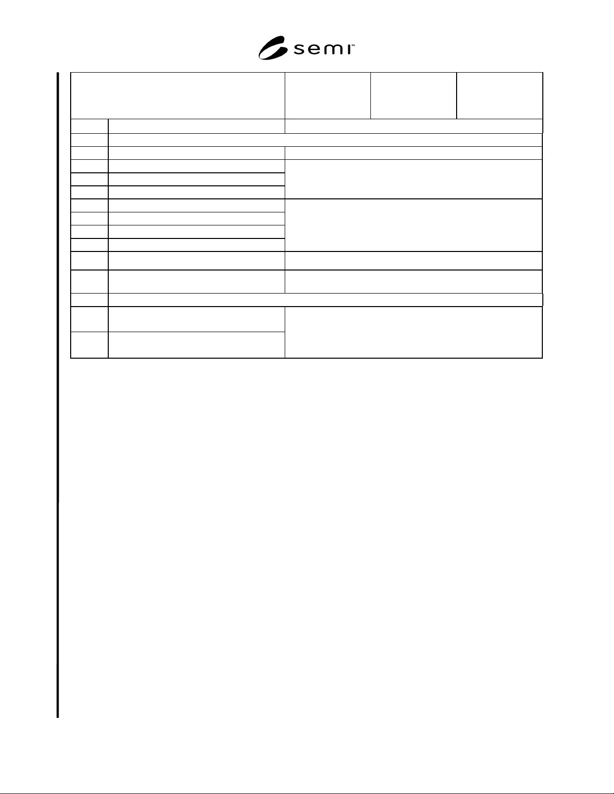
ITEM (See Note 1)
p/p
−
EPITAXIAL
WAFER
p/p
+
EPITAXIAL
WAFER
p/p
++
EPITAXIAL
WAFER
TDB Calcium
≤ 1 × 10
10
/cm
2
14.0
BACK SURFACE CRITERIA
14.1 Contamination/Area none
14.2 Scratches – macro
14.3 Scratches – micro
14.4 Localized Light Scatterers
supplier-purchaser agreement
TBD Edge Chips
TBD Cracks, Crow's Feet
TBD Saw Marks
TBD Stains
none
TBD Roughness Polished
TBD
Brightness (Gloss) 60° angle of incidence,
referenced to a mirror polished wafer.
≥ 80% (See Note 12)
15.0
OTHER CHARACTERISTICS
TBD
Denuded Zone
Free of Bulk Micro-defects (BMD)
TBD
BMD(Bulk Micro-defect Density)
Thermal Cycle per SEMI MF1239)
supplier-purchaser agreement
NOTE 1: The first column under item references SEMI Standard M18. M18 was in the process of substantial revision at the time this
documented was balloted. Many M18 line references remain to be determined. TBD is the abbreviation for “to be determined”.
NOTE 2: Unless otherwise agreed upon for a specific characteristic or test method.
NOTE 3: Only process control data is required. Data not required on Certificate of Compliance. A larger warp value may be appropriate if a
oxide layer is deposited on the back of the substrate.
NOTE 4: Oxygen level in itself should not be specified but rather is only a control parameter that may give an indication of the amount of
precipitation that will occur after some thermal process that nucleates and grows Bulk Micro-defects generated at precipitates. Addition of
nitrogen or carbon (above the background level) to the crystal can enhance the growth of these precipitates.
NOTE 5: Test in accordance with SEMI MF1188, JEIDA 61, or DIN 50438/1. Also see SEMI M44.
NOTE 6: Test in accordance with SEMI MF1366 or Gas Fusion Analysis, as agreed between supplier and purchaser. Non-destructive metrology
did not exist at the time this document was approved.
NOTE 7: Test in accordance with SEMI MF951, Plan A1, A2, or A3, as agreed between supplier and purchaser.
NOTE 8: Non-destructive metrology did not exist at the time this document was approved.
NOTE 9: The 9-point TTV parameter has been replaced by GBIR. See 12.4a.
NOTE 10: SFQR with a site size of 26 mm × 8 mm is approximately equal to SFSR with a site size of 26 mm x 32 mm at the 90 nm technology
level. The smaller site allows more coverage of the FQA than the larger site. The value of site flatness of 90 nm is taken from the ITRS Starting
Materials Table.
NOTE 11: The 90 nm count, 238, may be transformed to another maximum LLS count using draft international standard: ISO/DIS 14644-1
which uses the equation: count per wafer at 65 nm (new minimum size)
= (count per wafer at 90 nm)
*(90 nm / 65 nm)
2.
. For example
converting from a 90 nm minimum size to a 65 nm minimum size yields a count of 456.
NOTE 12: This specification implies a polished back surface.
NOTE 13: The intent in specifying carrier density using a range, rather than the center nominal with tolerance accompanied by a wafer variation
limit, is to minimize the importance of edge variations and to emphasize meeting the range of carrier density as it is allowed by the process and
the designers.
NOTE 14: Large Area Defects (LADs) are surface imperfections or particles that have geometry with at least one side or diameter that is equal to
or greater than the layer thickness. Their actual size cannot be currently implied from the output of an SSIS.
NOTE 15: Slip tested in accordance with SEMI MF1726; an etch depth < 100 nm is acceptable. The metrology used for slip determination is a
major factor in determining the presence or absence of slip lines. X-ray Topography is much more sensitive than the ASTM etching and
microscopic inspection method given here but no Standard Test Method currently exists. X-ray Topography will detect slip that may not
penetrate to the near surface region where the device is fabricated. Use of SSIS equipment set at less ≤90 nm can also reveal slip lines on epi
wafers but again no Standard Test Method currently exists. Surface roughness may interfere with SSIS measurements. With the thermal cycles
employed in 90 nm technology thermal processes, slip propagation should not be a problem.
NOTE 16: Value from the 2003 ITRS 90 nm node.
NOTE 17: May include stacking faults of different scattering intensities and other structural epitaxial defects which are not correctly sized by
current generation SSISs.

SEMI M11-0704 © SEMI 1988, 2004 35
NOTICE: SEMI makes no warranties or representations as to the suitability of the standards set forth herein for any
particular application. The determination of the suitability of the standard is solely the responsibility of the user.
Users are cautioned to refer to manufacturer’s instructions, product labels, product data sheets, and other relevant
literature respecting any materials mentioned herein. These standards are subject to change without notice.
The user’s attention is called to the possibility that compliance with this standard may require use of copyrighted
material or of an invention covered by patent rights. By publication of this standard, SEMI takes no position
respecting the validity of any patent rights or copyrights asserted in connection with any item mentioned in this
standard. Users of this standard are expressly advised that determination of any such patent rights or copyrights, and
the risk of infringement of such rights, are entirely their own responsibility.
Copyright by SEMI® (Semiconductor Equipment and Materials
International), 3081 Zanker Road, San Jose, CA 95134. Reproduction o
f
the contents in whole or in part is forbidden without express written
consent of SEMI.
SEMI M12-1103 © SEMI 1988, 2003 1
SEMI M12-1103
SPECIFICATION FOR SERIAL ALPHANUMERIC MARKING OF THE
FRONT SURFACE OF WAFERS
This specification was technically approved by the Global Traceability Committee and is the direct
responsibility of the North American Traceability Committee. Current edition approved by the North
American Regional Standards Committee on July 27, 2003. Initially available at www.semi.org October
2003; to be published November 2003. Originally published in 1988; previously published March 2003.
1 Purpose
1.1 This specification provides a serial alphanumeric
marking of silicon or other semiconductor wafers. The
wafer serial number links the properties of the wafer
stored in an appropriate database system to each
individual wafer for purposes of tracking and control
during wafer and device manufacture.
1.2 By defining the basic code used for the mark, this
specification ensures the consistency of wafer marking
performed by wafer manufacturers. Thus, it allows
simplification of the performance requirements of
automatic optical character reading (OCR) equipment,
provides for unassisted and immediate human
readability without wafer handling, and facilitates
resolution of wafer level process variations.
1.3 The marking code is intended to be valid for a
broad range of wafer products (i.e., epi, SOI, processed
polished wafers, etc.).
2 Scope
2.1 This specification defines the geometric and spatial
limits of the alphanumeric code, specifically for serial
identification of flatted and notched silicon wafers.
2.2 This specification does NOT address the marking
techniques that may be employed when complying with
this standard.
NOTICE: This standard does not purport to address
safety issues, if any, associated with its use. It is the
responsibility of the users of this standard to establish
appropriate safety and health practices and determine
the applicability of regulatory or other limitations prior
to use.
3 Referenced Standards
3.1 SEMI Standards
SEMI M13 — Specification for Alphanumeric Marking
of Silicon Wafers
NOTICE: Unless otherwise indicated, all documents
cited shall be the latest published versions.
4 Terminology
4.1 Definitions
4.1.1 adjacent character misalignment, R
adj
— the
vertical distance between the character baselines of two
adjacent characters on the same line.
4.1.2 character separation — the horizontal distance
between the adjacent boundaries of any two adjacent
characters.
4.1.3 character spacing — the horizontal distance
between the character centerlines of any two adjacent
characters.
4.1.4 character window — the rectangular window
within which all characters must be contained.
4.1.5 front surface of the wafer — the exposed surface
upon which active semiconductor devices have been or
will be fabricated.
4.1.6 line character misalignment, R
line
— the vertical
distance between the character baselines of the highest
and the lowest characters on the same line.
5 Shape and Size of Marking
5.1 Solid line or dot matrix method may be used to
write characters. The minimum matrix shall be 5 dots
horizontal and 9 dots vertical. More dots may be used,
up to and including a solid line. Higher density is
recommended to achieve improved read reliability (see
Related Information 1).
5.2 Character Dimensions and Spacing — (see Table 1
and Figure 1)
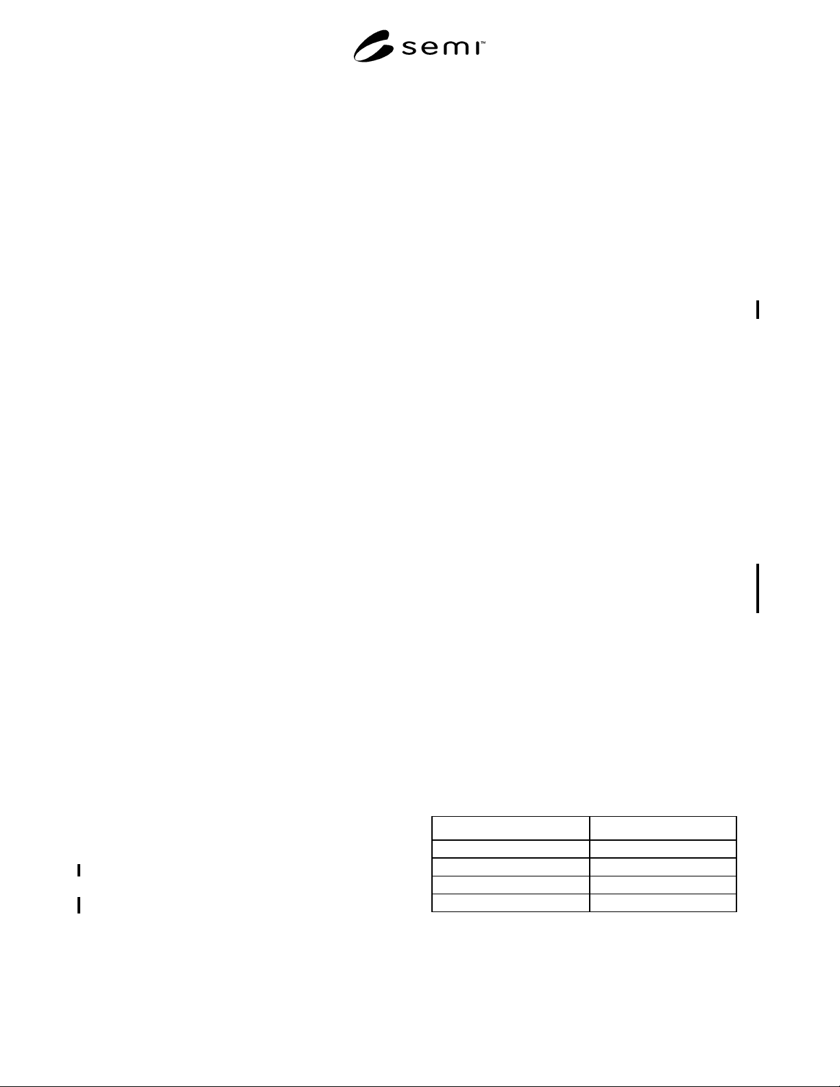
Table 1 Character Dimensions
Character mm
Height 1.624 ± 0.025
Width 0.812 ± 0.025
Thickness (See NOTE 1) 0.200 + 0.050/-0.150
Spacing 1.420 ± 0.025
NOTE 1: The thickness of the diagonal in the letter " N" is 0.138 ±
0.05 mm for single density dot matrix.