semi合集-English.pdf - 第4858页
SEMI M1-0305 © SEMI 1978, 2005 34 Item Specification 2-5. WAFER PREPARATION CHARACTERISTICS 2-5.1 Wafer ID Marking SEMI T7 plus op tional Alphanumeric Mark per Wafer Category 1.15 (see Figure 3) 2-5.7 Edge Surface Condit…
SEMI M1-0305 © SEMI 1978, 2005 33
6.8.2.9 Items 2-8.9b and 2-9.3b, crow’s feet—Any anomaly conforming to the definition that is greater than 0.25
mm (0.010 in. for 2 and 3 in. diameter wafers) in total length.
6.8.2.10 Item 2-8.10, craters—Any individually distinguishable surface anomaly conforming to the definition that is
visible when viewed under diffused illumination.
6.8.2.11 Item 2-8.11, dimples—Any smooth surface depression greater than 3 mm in diameter.
6.8.2.12 Item 2-8.12, grooves—Any anomaly conforming to the definition that is greater than 0.13 mm (0.0005 in.
for 2 in. and 3 in. diameter wafers) wide or 0.76 mm (0.030 in. for 2 in. and 3 in. diameter wafers) in length.
6.8.2.13 Item 2-8.13, mounds — Any anomaly conforming to the definition that is greater than 0.25 mm (0.010 in.
for 2 in. and 3 in. diameter wafers) in maximum dimension.
6.8.2.14 Item 2-8.14, orange peel — Any visually detectable roughened surface conforming to the definition that is
observable under diffused illumination.
6.8.2.15 Items 2-8.15 and 2-9.5, saw marks — Any anomaly conforming to the definition that is visible under
diffuse illumination.
6.8.2.16 Item 2-8.16, resistivity striations (dopant striation rings) — Any feature conforming to the definition that
is detectable under diffused lighting conditions.
6.8.3 For other cases, acceptable surface defect levels shall be defined based on the use of surface scanning
inspections systems (SSIS) for automated surface inspection. In this case, definitions of what surface anomalies
constitute surface defects shall be agreed upon between supplier and customer.
7 Basic Specification Requirements
7.1 A basic silicon wafer specification is one that describes a commercially appropriate prime silicon wafer product
having stable quality and parametric control. Wafers procured to this specification for 300 mm diameter, double
side polished silicon wafers shall meet all of the requirements of Table 11 without any change or additional options.
Listed specification values represent generally accepted silicon wafer process capability that is consistent with many
advanced integrated circuit applications at the 130 nm technology level.
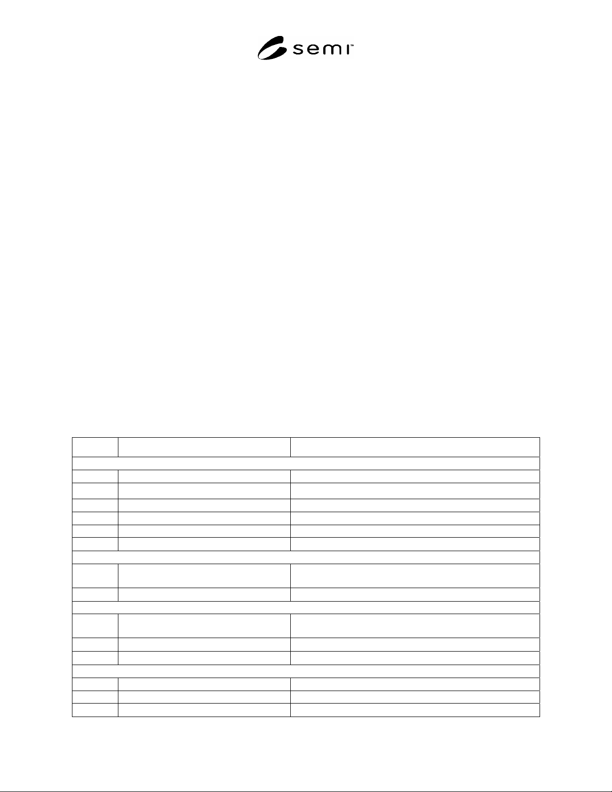
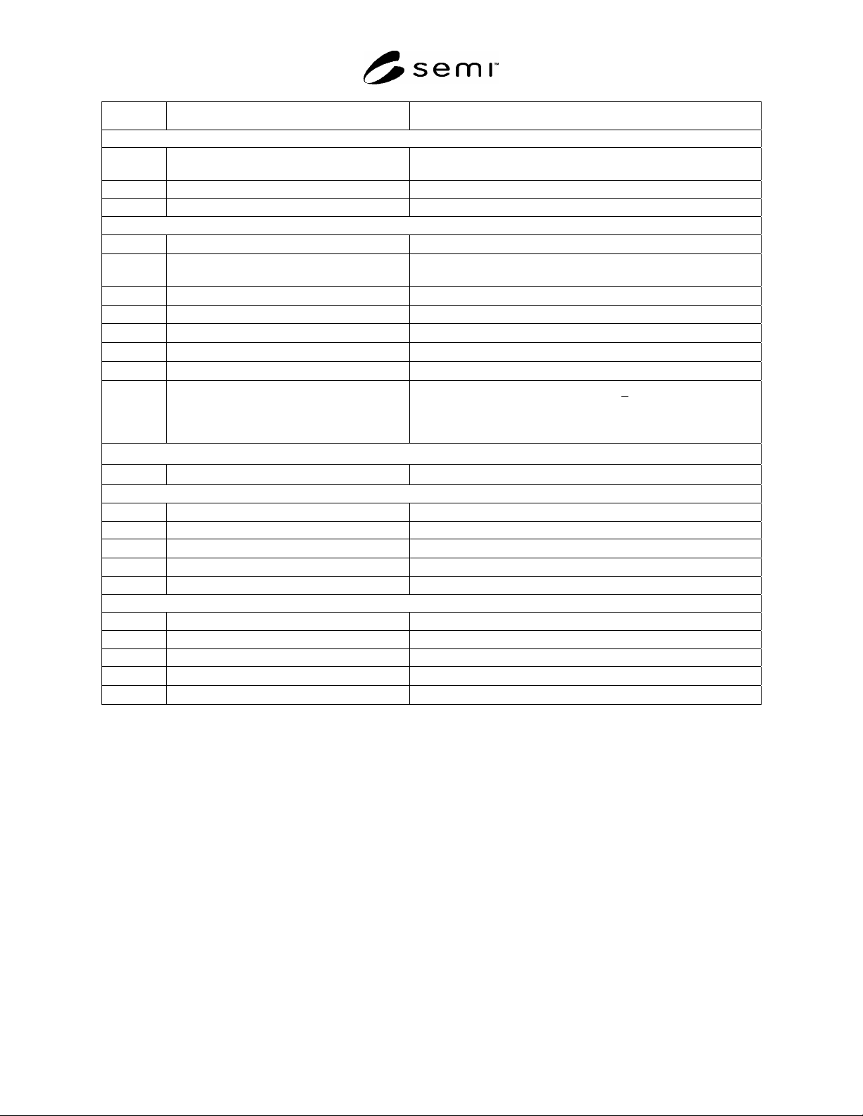
Table 11 Basic Specification for 300 mm Polished Prime Silicon Wafers for the 130 nm Technology Node
Item Specification
2-1. GENERAL CHARACTERISTICS
2-1.1 Growth Method Supplier Option of Cz or MCz
2-1.2
Use of Refined Polysilicon Permitted
2-1.4 Conductivity Type p
2-1.5 Dopant Boron
2-1.6 Nominal Edge Exclusion 3 mm
2-1.8
Wafer Surface Orientation
(100) 0.5
2-2. ELECTRICAL CHARACTERISTICS
2-2.1 Resistivity
Center Point (Target): 1.5 ·cm, 10 ·cm, or 21 ·cm
Resistivity Tolerance: 33%
2-2.2
Radial Resistivity Variation
10% at 6 mm from edge as in SEMI MF81, Sampling Plan B
2-3. CHEMICAL CHARACTERISTICS
2-3.1 Oxygen Concentration
Center Point (target): 15 or 18 ppma ( IOC-88)
Tolerance: 1.5 ppma (IOC-88)
2-3.2
Radial Oxygen Variation
10% at 10 mm from edge as in SEMI MF951, Sampling Plan A1
2-3.3
Carbon Concentration
0.5 ppma (SEMI MF1391)
2-4. STRUCTURAL CHARACTERISTICS
2-4.1 Dislocation Etch Pit Density None
2-4.2 Slip None
2-4.7
Oxidation Induced Stacking Faults
100 cm
2
SEMI M1-0305 © SEMI 1978, 2005 34
Item Specification
2-5. WAFER PREPARATION CHARACTERISTICS
2-5.1 Wafer ID Marking SEMI T7 plus optional Alphanumeric Mark per Wafer Category
1.15 (see Figure 3)
2-5.7 Edge Surface Condition Polished
2-5.8 Back Surface Condition Polished
2-6. DIMENSIONAL CHARACTERISTICS
2-6.1
Diameter
300.00 0.20 mm
2-6.2
Notch Dimensions In accordance with requirements of Wafer Category 1.15 (see Figure
5)
2-6.3
Notch Orientation
<110> 1
2-6.6 Edge Profile T/4 Template (see Figure 6)
2-6.7
Thickness
775 20 m
2-6.8
Total Thickness Variation (GBIR)
10 m
2-6.10
Warp
100 m
2-6.13 Site Flatness [SFQR]
#1
>99.9% of all full sites <200 nm;
Site size: 26 mm 8 mm
Include partial sites: No
Offset: None
2-7. FRONT SURFACE CHEMISTRY
2-7.1
Surface Metal Contamination
#2
1 10
10
cm
2
2-8. FRONT SURFACE INSPECTION CHARACTERISTICS
2-8.1 Scratches – macro None
2-8.2 Scratches – micro None
2-8.5
Localized Light Scatterers (LLS)
1200/wafer, 0.12m (LSE) and 10/wafer, 0.25m (LSE)
2-8.7 Edge Chips None
2-8.8 Edge Cracks None
2-9. BACK SURFACE INSPECTION CHARACTERISTICS
2-9.1 Edge Chips and Indents None
2-9.2 Edge Cracks None
2-9.4 Area Contamination None
2-9.9
Scratches macro <0.25 Diameter
2-9.10
Scratches micro
Not Specified
#1
This site flatness process capability allows approximately one full site to have SFQR >200 nm for every four wafers shipped.
#2
Individual process median capability for each of the following metal contaminants: Al, Ca, Cr, Cu, Fe, K, Na, Ni, and Zn. Due to high
measurement variability, data are recorded for process capability and not for individual shipment quality reports.
7.2 Effective implementation of the basic specification concept requires the standardization of many wafer
characteristics that have not historically been specified in a SEMI standard, as well as some characteristics that have
historically been specified in SEMI standards, but have been routinely modified as a customer preference. The
resulting variety of customer specifications causes silicon suppliers to install additional processes and metrics, or
different processes and technologies for satisfying individual specifications. To realize the full benefits of a basic
specification, it is essential that all parameters be accepted without additional options.
7.3 Wafers produced to this specification shall be qualified through routine process checks, demonstrating the
process is in state of control. Verification of the process and quality control shall be provided on a shipment basis
through a certification that does not require the inclusion of data specifically from that shipment.

SEMI M1-0305 © SEMI 1978, 2005 35
8 Sampling
8.1 Unless otherwise specified, ASTM Practice E 122 shall be used to define the sampling plan. When so specified,
appropriate sample sizes shall be selected from each lot in accordance with ANSI/ASQC Z1.4. Each quality
characteristic shall be assigned an acceptable quality level (AQL) or lot tolerance percent defective (LTPD) value in
accordance with ANSI/ASQC Z1.4 definitions for critical, major, and minor classifications. If desired and so
specified in the contract or order, each of these classifications may alternatively be assigned cumulative AQL or
LTPD values. Inspection levels shall be agreed upon between the supplier and the purchaser.
9 Test Methods
9.1 Measurements shall be made or certifiable to one of the SEMI, ASTM, JEITA, JIS, or DIN standard test
methods for the item as selected from Table 1 and specified in the purchase order.
9.2 If several different standard test methods for an item are commonly used within a region, it is particularly
important that the applicable method of test be identified in the purchase order.
9.3 If no method of test is specified in the purchase order and if standard test methods from different geographic
regions are available, the default method shall be a method in common usage for the region of the purchaser of the
wafer.
9.4 If no standard test method for an item is available, the test procedure to be used must be agreed upon between
supplier and customer.
9.5 Information about the various test methods listed in Table 1 is provided in Related Information 2 together with
information about some additional test methods no longer in wide use throughout the industry.
10 Certification
10.1 Upon request of the purchaser in the contract or order, a manufacturer’s or supplier’s certification that the
material was manufactured and tested in accordance with this specification, together with a report of the test results,
shall be furnished at the time of shipment.
10.2 In the interest of controlling inspection costs, the supplier and the customer may agree that the material shall
be certified as “capable of meeting” certain requirements. In this context, “capable of meeting” shall signify that the
supplier is not required to perform the appropriate tests in §9. However, if the customer performs the test and the
material fails to meet the requirement, the material may be subject to rejection.
11 Product Labeling
11.1 The wafers supplied under these specifications shall be identified by appropriately labeling the outside of each
box or other container and each subdivision thereof in which it may reasonably be expected that the wafers will be
stored prior to further processing. Identification shall include as a minimum the nominal diameter, conductivity
type, dopant, orientation, resistivity range, and lot number. The lot number, either (1) assigned by the original
manufacturer of the wafers, or (2) assigned subsequent to wafer manufacture but providing reference to the original
lot number, shall provide easy access to information concerning the fabrication history of the particular wafers in
that lot. Such information shall be retained on file at the manufacturer’s facility for at least one month after that
particular lot has been accepted by the customer.
11.2 Alternatively, if agreed upon between supplier and customer, one of the box labeling schemes in SEMI T3
shall be used and the information listed in ¶11.1 that is not included on the label shall be retained in the supplier’s
data base for at least one month after that particular lot has been accepted by the customer.
11.3 Wafers of Category 1.15 (300 mm in diameter) shall be shipped in packages labeled in accordance with SEMI
M45.