semi合集-English.pdf - 第4854页
SEMI M1-0305 © SEMI 1978, 2005 30 Table 9 Dimensional Characteristic s and Wafer ID Marking Requiremen ts for Notched 200 mm and 300 mm Polished Monocrys ta lline Silicon Wafers #1 Previous SEMI Refer ence: SEMI M1.9 SEM…
SEMI M1-0305 © SEMI 1978, 2005 29
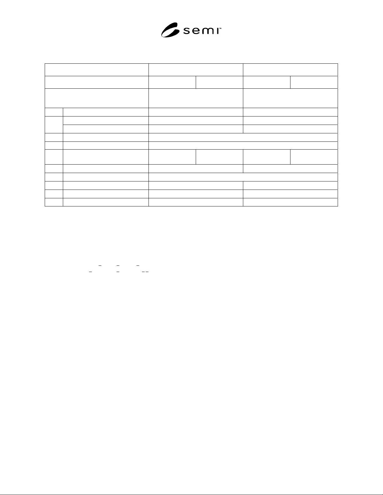
Table 8 Dimensional Characteristics of 150 mm and 200 mm Polished Monocrystalline Silicon Wafers
without Secondary Flat
#1
Previous SEMI Reference: SEMI M1.13 SEMI M1.10
Wafer Category: 1.13.1 1.13.2 1.10.1 1.10.2
Property
150 mm Wafers without secondary flat
(t=625
m)
#2
200 mm Wafers flatted, without
secondary flat
#2
2-6.1 Diameter
150.00 0.20 mm 200.00 0.20 mm
Primary Flat Length
47.5 2.5 mm
Not applicable 2-6.2
Flat Diameter Not applicable
195.50 0.20 mm
2-6.3 Primary Flat Orientation
#3
{110} 1
2-6.5 Secondary Flat Location No secondary flat
2-6.6 Edge Profile Coordinate,
C
y
(see Table 3)
T/3 Template
208 m
T/4 Template
156 m
T/3 Template
242 m
T/4 Template
181 m
2-6.7 Thickness, Center Point
625 15 m 675 15 m
2-6.8 Total Thickness Variation, Max.
10 m
2-6.9 Bow, Max.
60 m 65 m
2-6.10 Warp, Max.
60 m 75 m
2-5.7 Edge Surface Condition Not specified Supplier-customer agreement
#4
#1
Note that these specifications were originated in Japan. They are equivalent to the specifications for wafers of the same nominal diameter in
JEITA EM-3602. Care should be taken in applying this configuration to specific applications (see ¶6.6.3).
#2
For referee purposes, metric (SI) units apply. To ensure that product shipped is within specification, any conversion to U.S. Customary
equivalents should be done following the maximum-minimum convention in which the minimum values are rounded-up and the maximum values
are rounded-down to ensure that the equivalent range is always inside the referee range. If U.S. Customary equivalents are used for incoming
inspection, minimum values should be rounded-down and maximum values rounded-up to avoid rejection of material that is within the
specification when measured by the referee system of units. CAUTION: The significance of the rightmost digit may vary, depending on the
quantity being measured and the precision of the test procedure. Refer to the relevant test method for precision data which can be used to
construct appropriate guard bands.
#3
For )111( wafers, the
),011( ),101( and )011( planes are the equivalent, allowable (110) planes. For (100) wafers, the allowable equivalent
)110( planes are
),101(),011( ),110( and ).110(
#4
If specified as polished, this term is meant to imply a surface condition and not a particular processing technique. If desired, a quantitative
measure of surface finish may optionally be indicated by specifying the rms microroughness over a specified spatial frequency (or wavelength)
range. Because a standardized test method has not yet been developed for this metric, both values and test procedures, including sampling plan
and detrending procedures, shall be agreed upon between supplier and customer.
SEMI M1-0305 © SEMI 1978, 2005 30
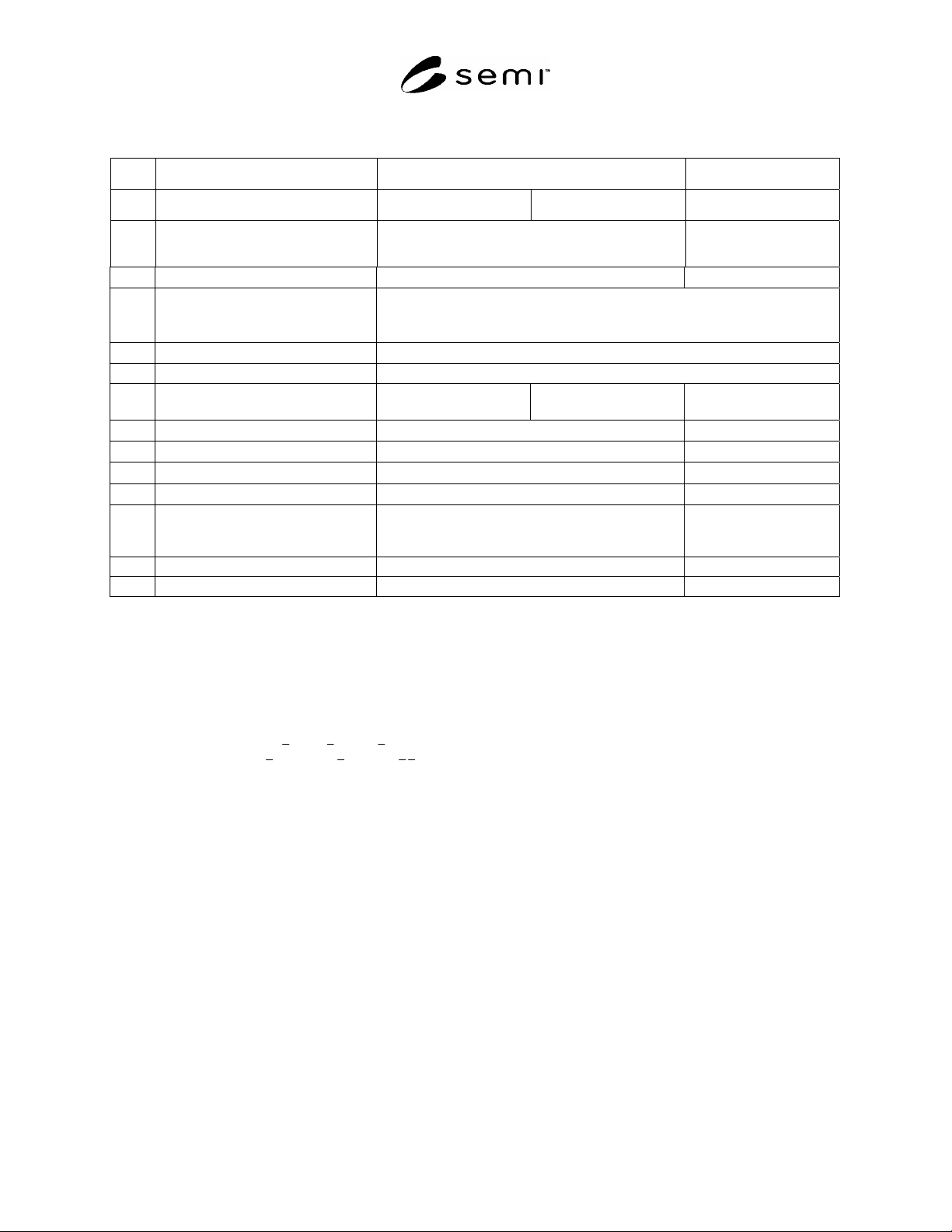
Table 9 Dimensional Characteristics and Wafer ID Marking Requirements for Notched 200 mm and 300 mm
Polished Monocrystalline Silicon Wafers
#1
Previous SEMI Reference: SEMI M1.9 SEMI M1.15
Wafer Category: 1.9.1 1.9.2 1.15
Property 200 mm Wafers (Notched)
#2
300 mm Wafers
(Notched)
#2
2-6.1 Diameter
200.00 0.20 mm. 300.00 0.20 mm
2-6.2 Notch Dimensions (See Figure 5)
Depth
Angle
1.00 mm +0.25 mm 0.00 mm
90 +5 1
2-6.3 Orientation of Notch Axis
#3
<110> 1
2-6.5 Secondary Fiducial Location No secondary fiducial
2-6.6 Edge Profile Coordinate,
C
y
(see Table 3)
T/3 Template
242 m
T/4 Template
181 m
T/4 Template
194 m
2-6.7 Thickness, Center Point
725 20 m. 775 20 m
2-6.8 Total Thickness Variation, Max.
10 m 10 m
#4
2-6.9 Bow, Max.
65 m
Not specified
2-6.10 Warp, Max.
75 m 100 m
#5
2-5.1 Wafer ID Marking Supplier-customer agreement SEMI T7 mark with
optional A/N mark (See
¶6.5.1.4)
2-5.7 Edge Surface Condition
Supplier-customer agreement
#6
Polished
#6
2-9.8 Back Surface Brightness (Gloss) Not specified 0.80
#6,#7
#1
Note that these specifications were originated in the United States. Care should be taken in applying this configuration to specific applications
(see ¶6.6.3). The specification for 300 mm wafers is essentially equivalent to the specification for wafers of this diameter in JEITA EM-3602.
#2
For referee purposes, metric (SI) units apply. To ensure that product shipped is within specification, any conversion to U.S. Customary
equivalents should be done following the maximum-minimum convention in which the minimum values are rounded-up and the maximum values
are rounded-down to ensure that the equivalent range is always inside the referee range. If U.S. Customary equivalents are used for incoming
inspection, minimum values should be rounded-down and maximum values rounded-up to avoid rejection of material that is within the
specification when measured by the referee system of units. CAUTION: The significance of the rightmost digit may vary, depending on the
quantity being measured and the precision of the test procedure. Refer to the relevant test method for precision data which can be used to
construct appropriate guard bands.
#3
For 200 mm )111( wafers, the
],011[ ],101[ , and ]011[ axes are the equivalent, allowable <110> axees. For (100) wafers, the allowable
equivalent <110> axes are
],101[
],011[
],110[
and
].110[
#4
Full wafer scan as described in SEMI MF1530.
#5
Warp corrected for gravitational effects. However, warp is not an adequate wafer shape specification for all applications.
#6
If specified as polished, this term is meant to imply a surface condition and not a particular processing technique. If desired, a quantitative
measure of surface finish may optionally be indicated by specifying the rms microroughness over a specified spatial frequency (or wavelength)
range. Because a standardized test method has not yet been developed for this metric, both values and test procedures, including sampling plan
and detrending procedures, shall be agreed upon between supplier and customer.
#7
Gloss as measured in accordance with ASTM Test Method D 523 or JIS Z 8741 with visible illumination at a 60° angle of incidence referenced
to a mirror polished silicon wafer front surface. This metric may not describe the back surface finish adequately to establish detectability of small
localized light scatterers (LLSs). If it is necessary to detect LLSs smaller than 0.25 µm LSE, another quantitative measure of surface finish may
optionally be indicated by specifying the rms microroughness over a specified spatial frequency (or wavelength) range. Because a standardized
test method has not yet been developed for this metric, both values and test procedures shall be agreed upon between supplier and customer.

SEMI M1-0305 © SEMI 1978, 2005 31
6.6.3 Shape — The shape decision tree in Appendix 2 fully describes the various shape parameters that can be
specified.
6.6.3.1 Warp is generally the most often specified shape parameter. Only wafers of category 1.1 (2 in. diameter) do
not have a warp specification. Note that there are two forms of warp, one corrected for gravitational sag and the
other not so corrected.
6.6.3.2 If bow is specified, a sign may be included in the specification to denote convex (positive) or concave
(negative) curvature of the median surface of the wafer with the front surface up. If no sign is included in the
specification, bow may vary between -a and +a, where “a” is the specified maximum magnitude of bow.
6.6.3.3 Sori is an attribute that may be specified with agreement between the supplier and customer in lieu of or in
addition to bow and/or warp.
6.6.4 Standard Wafer Categories — The standardized dimensions, dimensional tolerances, and fiducial (flat or
notch) characteristics for various standard wafer categories are summarized in Tables 4 through 9. These categories
of wafers shall meet all requirements listed in the appropriate table, unless an exception is negotiated between
supplier and customer and is shown on the purchase order.
6.6.4.1 Wafers of the same nominal diameter may typically have different dimensional configurations in different
regions of the world. Many of these configurations are represented in these tables. In selecting the appropriate
standard polished wafer category, consideration should be given to compatibility with processes and equipment
generally available in the region of use.
6.6.5 Flatness — The wafers shall meet global and site flatness requirements as specified in the purchase order.
Details of different flatness parameters are given in Appendix 1.
6.6.6 Nanotopography — The wafers shall meet nanotopography requirements specified in the purchase order.
6.7 Front Surface Chemistry
6.7.1 If surface metal contamination levels are specified on the purchase order, the maximum area densities shall be
designated in units of atoms/cm
2
for specific individual elements together with the measurement method by which
the densities are to be determined. The wafers shall not contain more than the specified density of each metal.
NOTE 3: An example of such a specification applicable to 1 m geometries is given in Related Information 1.
6.7.2 If surface organic contamination levels are specified on the purchase order, the maximum area densities shall
be designated in units of ng/cm
2
for total surface organics density together with the method by which the density is
to be determined. The wafers shall not contain more than the specified density of total surface organics.
6.8 Front and Back Surface Inspection Characteristics
6.8.1 The wafers shall conform to the limits on observable (visually or otherwise) front and back surface
characteristics as specified on the purchase order.
6.8.2 For wafers of diameter 150 mm or smaller for which visual inspection of surface defects is acceptable, the
defect limits in Table 10 may be used as a guide for determining acceptable defect levels. Under these
circumstances, minimal conditions or dimensions for surface features to be considered as defects are stated below.
These limits shall be used for determining wafer acceptability; anomalies smaller than these limits shall not be
considered defects.
6.8.2.1 Item 2-8.1, scratches, macro — Any anomaly conforming to the definition that has a length-to-width ratio
greater than 5:1 and is visible under diffuse illumination as well as under high intensity illumination.
6.8.2.2 Item 2-8.2, scratches, micro — Any anomaly conforming to the definition that has a length-to-width ratio
greater than 5:1 and is visible only under high intensity illumination.
6.8.2.3 Item 2-8.3, pits — Any individually distinguishable nonremovable surface anomaly conforming to the
definition that is visible when viewed under intense illumination.
6.8.2.4 Item 2-8.4, haze — Haze is indicated when the image of a narrow beam tungsten lamp filament is detectable
on the polished wafer surface. Under some conditions, contamination may appear as haze.