semi合集-English.pdf - 第5882页
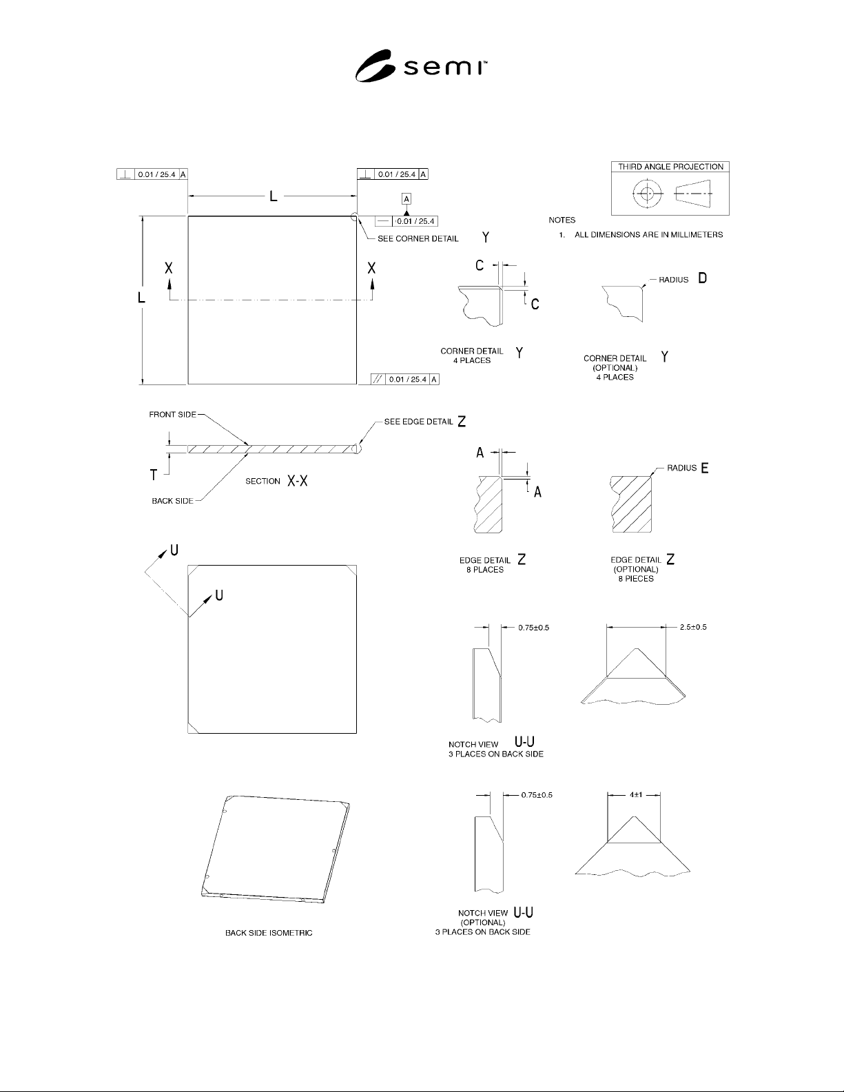
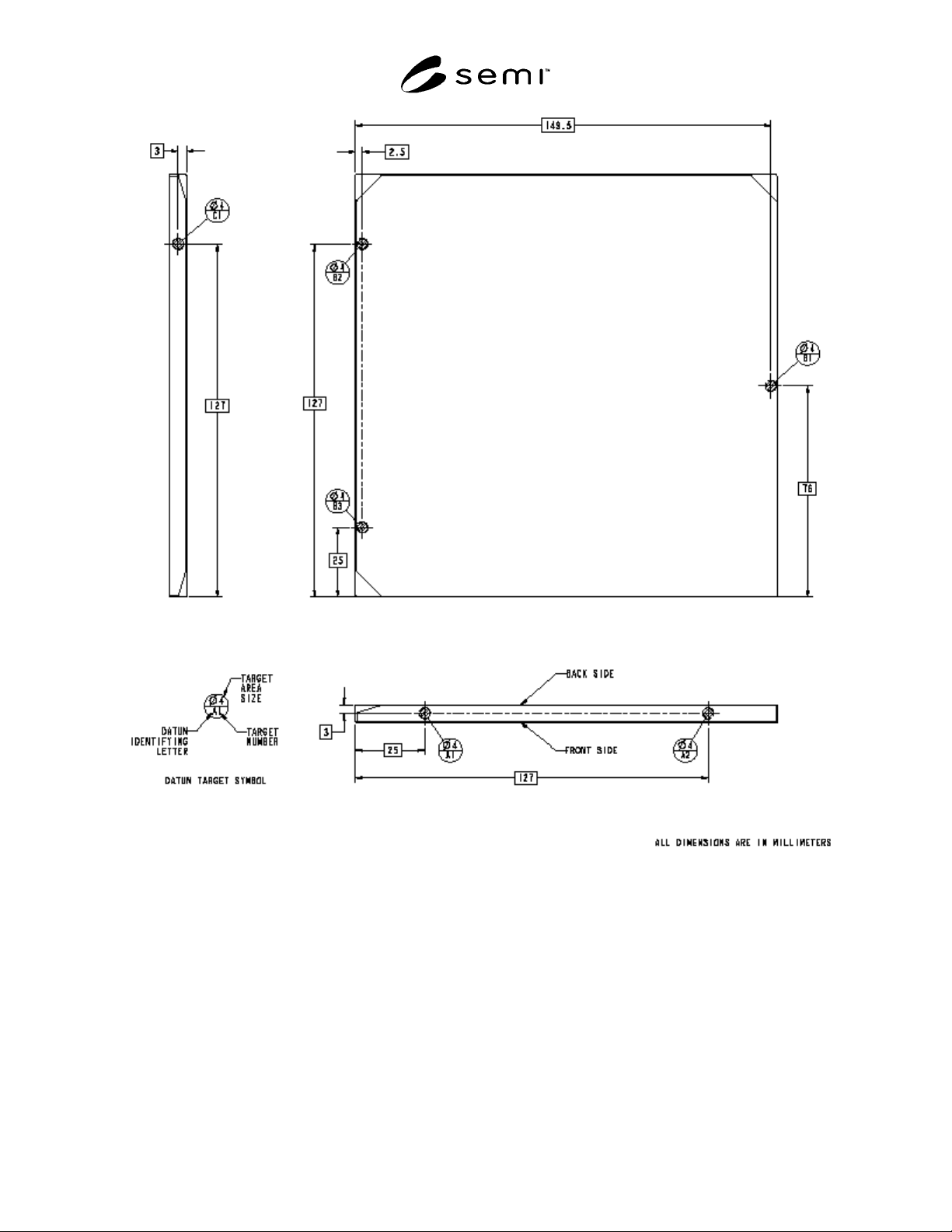
SEMI P37-1102 © SEMI 2001, 2002 4 Figure 2 Datum locati ons on the E UVL mask subs trate
SEMI P37-1102 © SEMI 2001, 2002 3
13.2 Containers shall be labeled “Warning: Open and Handle Under Cleanroom Conditions Only” as well as
identified by user purchase order number (if applicable), drawing number (if applicable), quantity, supplier lot
number, and material identification.
Figure 1
Dimensions of EUVL mask substrate
SEMI P37-1102 © SEMI 2001, 2002 4
Figure 2
Datum locations on the EUVL mask substrate
SEMI P37-1102 © SEMI 2001, 2002 5
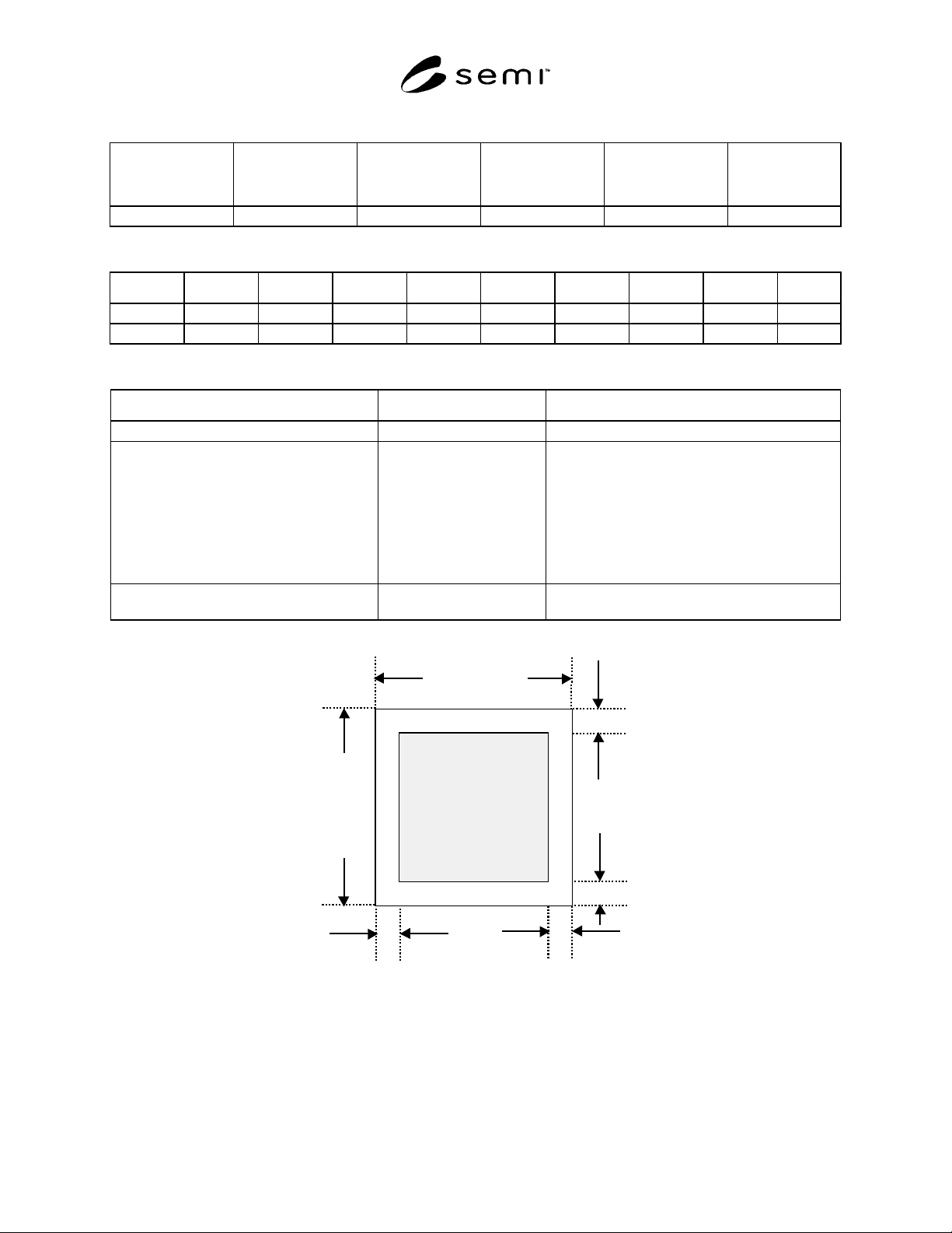
Table 1 Specifications for Edge Length, Squareness, and Thickness for Square Substrates
Edge Length Min.
L
Edge Length Max.
L
Squareness
Minimum Mean
Thickness
T
Maximum Mean
Thickness
T
Units
151.9 152.1 0.01/25.40 6.25 6.45 mm
Table 2 Specifications for Chamfered and Rounded Edge Dimensions
T A A C C D D E E
Nominal Min. Max. Min. Max. Min. Max. Min. Max. Units
6.35 0.20 0.30 0.30 0.70 0.50 1.00 0.25 0.30 mm
Table 3 Substrate Material Characteristics
Property Symbol Characteristic
Temperature range for CTE requirement 19 to 25°C
Coefficient of Thermal Expansion CTE (ppb/°C)
Class A: mean: 0 ± 5 ppb/°C
6 ppb/°C total spatial variation
Class B: mean: 0 ± 10 ppb/°C
10 ppb/°C total spatial variation
Class C: mean: 0 ± 20 ppb/°C
10 ppb/°C total spatial variation
Class D: mean: 0 ± 30 ppb/°C
10 ppb/°C total spatial variation
Specific Stiffness (Young’s elastic modulus
divided by density)
Ε/ρ (m
2
s
-2
)
≥ 3 × 10
7
Note: ppb stands for parts per billion.
5 mm
Flatness
quality
area
Edge Length
Edge Length
5 mm
5 mm5 mm
Figure 3
Front and Back Side Flatness Quality Area