semi合集-English.pdf - 第189页
SEMI E23-1104 © SEMI 1991, 2004 7 Table 6 Pin Assignment for Wire-Conn ected Parallel I/O Interface 15 Pins Connector Pin No. Signal Pin No. Signal 1 CS1 L_REQ 9 CS1 L_REQ* 2 CS1 U_REQ 10 CS1 U_REQ* 3 CS1 READY 11 CS1 RE…
SEMI E23-1104 © SEMI 1991, 2004 6
6 Connector and Interface Circuit
6.1 Wire-Connected Interface — One set of connectors
is provided for the CS’s that commonly input the
BUSY and COMPT signals.
6.1.1 Connector and Pin Assignment
1. Connector JIS-X-5103 (D-SUB type) ISO-4902
Every piece of equipment is to have female type
connectors.
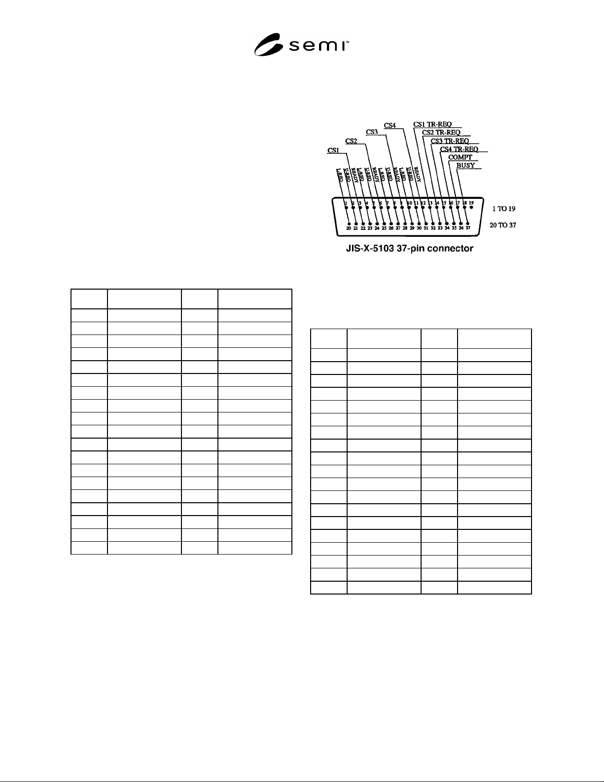
2. Pin Assignment — The connector with 37 pins is
used. One connector is used for 1 to 4 cassette
stages and another connector is used for 5 to 7
cassette stages. The pin assignment is listed in
Tables 4a and 4b. Figure 5 shows the pin
assignment of the connector for 4 cassette stages.
Table 4 Pin Assignment for Wire-Connected Parallel
I/O Interface (Connector 2)
Pin No. Signal Pin No. Signal
1 CS1 L_REQ 20 CS1 L_REQ*
2 CS1 U_REQ 21 CS1 U_REQ*
3 CS1 READY 22 CS1 READY*
4 CS2 L_REQ 23 CS2 L_REQ*
5 CS2 U_REQ 24 CS2 U_REQ*
6 CS2 READY 25 CS2 READY*
7 CS3 L_REQ 26 CS3 L_REQ*
8 CS3 U_REQ 27 CS3 U_REQ*
9 CS3 READY 28 CS3 READY*
10 CS4 L_REQ 29 CS4 L_REQ*
11 CS4 U_REQ 30 CS4 U_REQ*
12 CS4 READY 31 CS4 READY*
13 CS1 TR_REQ 32 CS1 TR_REQ*
14 CS2 TR_REQ 33 CS2 TR_REQ*
15 CS3 TR_REQ 34 CS3 TR_REQ*
16 CS4 TR_REQ 35 CS4 TR_REQ*
17 COMPT 36 COMPT*
18 BUSY 37 BUSY*
19 38
*Vcc side (power source) for the current-driven type circuit. Common
side for the voltage-driven type circuit.
6.1.1.1 When one connector is used for only one
cassette stage, the connector with 15 pins may be used.
The pin assignment is listed in the Table 5.
6.1.2 Interface Circuit — The following two types of
interface circuits are used. (Interface circuit examples
are shown in Related Information 3.)
1. Voltage-driven Type Circuit — Driving voltage:
DC24 ± 2 V
2. Current-driven Type Circuit — Driving current: 10
mA ~ 20 mA
Figure 5
Pin Assignment for Wire-Connected Parallel I/O
Interface
Table 5 Pin Assignment for Wire-Connected
Parallel I/O Interface (Connector 1)
Pin No. Signal Pin No. Signal
1 CS5 L_REQ 20 CS5 L_REQ*
2 CS5 U_REQ 21 CS5 U_REQ*
3 CS5 READY 22 CS5 READY*
4 CS6 L_REQ 23 CS6 L_REQ*
5 CS6 U_REQ 24 CS6 U_REQ*
6 CS6 READY 25 CS6 READY*
7 CS7 L_REQ 26 CS7 L_REQ*
8 CS7 U_REQ 27 CS7 U_REQ*
9 CS7 READY 28 CS7 READY*
10 29
11 30
12 31
13 CS5 TR_REQ 32 CS5 TR_REQ*
14 CS6 TR_REQ 33 CS6 TR_REQ*
15 CS7 TR_REQ 34 CS7 TR_REQ*
16 35
17 36
18 37
19
*Vcc side (power source) for the current-driven type circuit. Common
side for the voltage-driven type circuit.
SEMI E23-1104 © SEMI 1991, 2004 7
Table 6 Pin Assignment for Wire-Connected Parallel
I/O Interface 15 Pins Connector
Pin No. Signal Pin No. Signal
1 CS1 L_REQ 9 CS1 L_REQ*
2 CS1 U_REQ 10 CS1 U_REQ*
3 CS1 READY 11 CS1 READY*
4 12
5 CS1 TR_REQ 13 CS1 TR_REQ*
6 COMPT 14 COMPT*
7 BUSY 15 BUSY*
8
*Vcc side (power source) for the current-driven type circuit. Common
side for the voltage-driven type circuit.
6.2 Photo-Coupled Interface
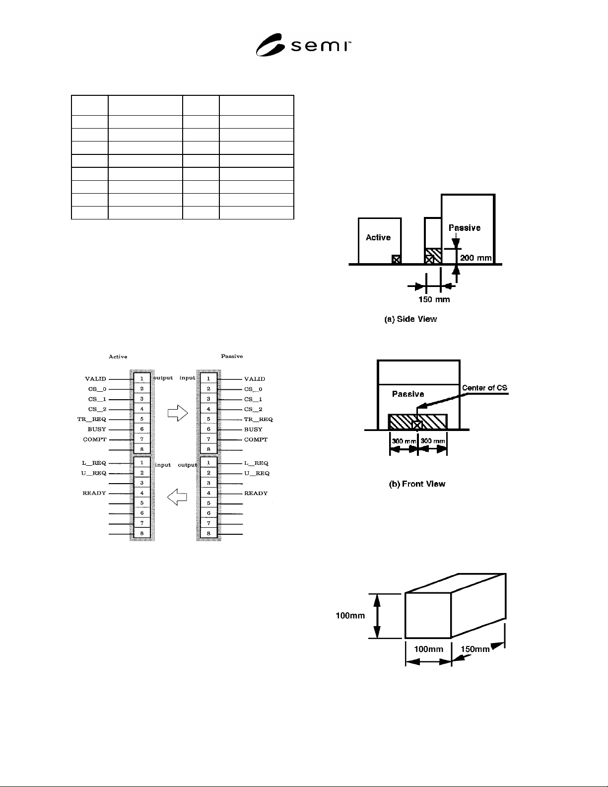
6.2.1 Photo-Coupled Device and Bit Assignment — To
date, there is no applicable documentor standard for
photo-coupled devices. This defines the usage of a
photo-coupled device of 8 bit-input/8 bit-output two-
way communications type. The bit assignment is shown
in Figure 6.
Figure 6
Bit Assignment of Photo-Coupled Device for the
Photo-Coupled Parallel I/O Interface
7 Installation Space
7.1 Wire-Connected Interface — Not specified.
7.2 Photo-Coupled I/O Interface — The photo-coupled
I/O interface must be located within the hatched area
indicated in Figure 7.
Figure 7
Installation Space of Photo-Coupled I/O inter-
face
Figure 8
Maximum Size of Photo-Coupled I/O Interface
SEMI E23-1104 © SEMI 1991, 2004 8
RELATED INFORMATION 1
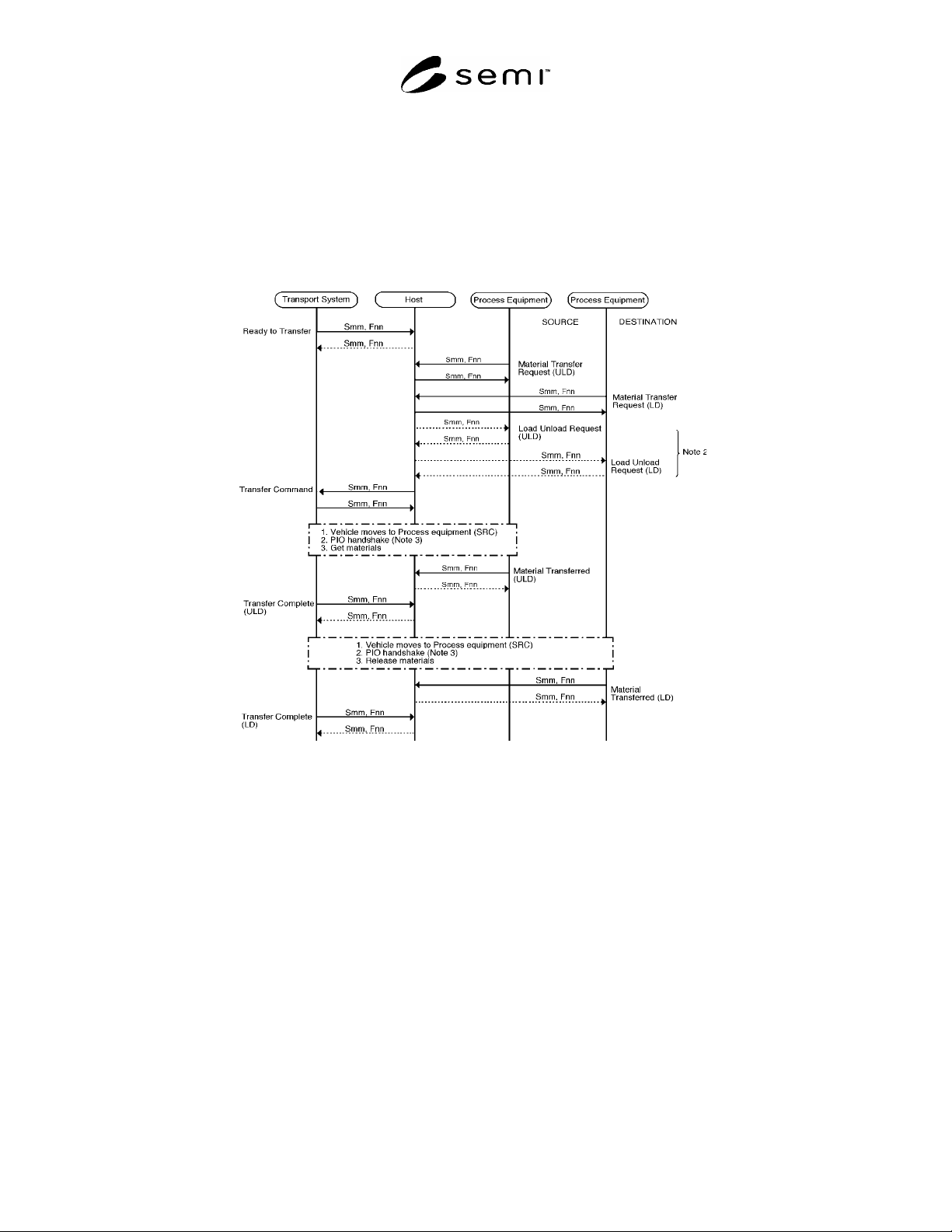
EXAMPLE OF A CASSETTE TRANSFER TRANSACTION USING THE
PARALLEL I/O INTERFACE
NOTICE: This example of a cassette transfer transaction using the parallel I/O interface is not an official part of this document
and is not intended to modify or supercede the official standard. Determination of the suitability of the material is solely the
responsibility of the user.
Figure R1-1
Example of a Cassette Transfer Transaction Using the Parallel I/O Interface
R1-1 NOTES
R1-1.1 LD = load, ULD = unload.
R1-1.2 The load/unload request (Smm, Fnn) may be eliminated if the material transfer request (Smm, Fnn) issued
after the materials have been prepared on the specified port for unloading or specified port has been readied for
loading.
R1-1.3 Multiple PIO handshakings may be required if material transfer request message (Smm, Fnn) has multiple
MID’s and PIN’s for multiple material transfers. MID: Material ID, PIN: Port number.
R1-1.4 The dotted line means optional message.
R1-1.5 In the future, the appropriate specific SECS-II message may be assigned for above Smm, Fnn message,
respectively.