semi合集-English.pdf - 第5183页
SEMI M34-0299 © SEMI 1999 1 SEMI M34-0299 GUIDE FOR SPECIFYING SIMOX WAFERS 1. Purpose 1.1 This guide is for speci fication of SIMOX (separation by implanta tion of oxygen ) wafers with less than 0.5 µ m sili con film th…

SEMI M33-0998 © SEMI 19989
Furukawa, Advanced in X-ray Analytic Japan, 26s, 19–
24, 1995
Statistical Process Control in Microelectronics
Manufacturing — W. A. Levinson, Semiconductor
International, 1994 November, pp. 95–102
Sub-ppm Monitoring of Transition Metal
Contamination on Silicon Wafer Surfaces by VPD-
TXRF
— A. Huber, H. J. Rath, P. Eichinger, T. Bauer,
L. Kotz, and R. Staudigl, PV 88–20, The
Electrochemical Society, 1988, p. 109
Theory of Analytical Chemistry — K.S. Booksh and B.
R. Kowalski, Journal Analytical Chemistry 66A (15),
782–91, 1994
Trace-Analytical Methods for Monitoring
Contamination in Semiconductor-Grade Si
Manufacturing — L. Fabry, S. Pahlke, L. Kotz, and G.
Tölg Fresenius Journal Analytical Chemistry, 349, 260–
71, 1994
TXRF in the Daily Routine — L. Fabry, S. Pahlke, L.
Kotz, E. Schemmel, and W. Berneike, PV 93–15, The
Electrochemical Society, 1993, pp. 232–9
Ultra-Trace Analysis of Metallic Contamination on
Silicon Wafer Surfaces by Vapor Phase
Decomposition/Total Reflection X-Ray Fluorescence
(VPD/TXRF)
— C. Neumann and P. Eichinger,
Spectrochimica, Acta 46B (19), 1360–77, 1991
Verfahren Zum Schutz Von Polierten Oberflächen — I.
Lampert, Europe Patent 0 222 400 (11/13/86)
NOTICE: These standards do not purport to address
safety issues, if any, associated with their use. It is the
responsibility of the user of these standards to establish
appropriate safety and health practices and determine
the applicability of regulatory limitations prior to use.
SEMI makes no warranties or representations as to the
suitability of the standards set forth herein for any
particular application. The determination of the
suitability of the standard is solely the responsibility of
the user. Users are cautioned to refer to manufacturer’s
instructions, product labels, product data sheets, and
other relevant literature respecting any materials
mentioned herein. These standards are subject to
change without notice.
The user’s attention is called to the possibility that
compliance with this standard may require use of
copyrighted material or of an invention covered by
patent rights. By publication of this standard, SEMI
takes no position respecting the validity of any patent
rights or copyrights asserted in connection with any
item mentioned in this standard. Users of this standard
are expressly advised that determination of any such
patent rights or copyrights, and the risk of infringement
of such rights, are entirely their own responsibility.
Copyright by SEMI® (Semiconductor Equipment and Materials
International), 3081 Zanker Road, San Jose, CA 95134. Reproduction o
f
the contents in whole or in part is forbidden without express written
consent of SEMI.

SEMI M34-0299 © SEMI 1999 1
SEMI M34-0299
GUIDE FOR SPECIFYING SIMOX WAFERS
1. Purpose
1.1 This guide is for specification of SIMOX
(separation by implantation of oxygen) wafers with less
than 0.5 µm silicon film thickness used for
semiconductor device manufacture. These speci-
fications define the generic characteristics of SIMOX
SOI wafers; the specific values for measured
parameters will be determined by agreement between
the user and supplier for the application. By defining
parameters, inspection procedures, and acceptance
criteria, both users and suppliers may uniformly define
product characteristics and quality requirements.
2. Scope
2.1 The primary standardized properties set forth in
this specification relate to physical and electrical
characteristics of SIMOX wafers.
3. Referenced Documents
3.1 SEMI Standards
SEMI M1 — Specifications for Polished Mono-
crystalline Silicon Wafers
SEMI M22 — Specification for Dielectrically Isolated
(DI) Wafers
3.2 ASTM Documents
1
Practice E 122 (vol. 14.02) — Practice for Choice of
Sample Size to Estimate Average Quality of a Lot or
Process
F 154 (vol. 10.05) — Standard Practices and
Nomenclature for Indentification of Structures and
Contaminants Seen on Specular Silicon Surfaces
F 523 (vol. 10.05) — Standard Practice for Unaided
Visual Inspection of Polished Silicon Slices
3.3 Other Standards
2
ANSI/ASQC Z1.4 — Sampling Procedures and Tables
for Inspection by Attributes
1 American Society for Testing and Materials, 100 Barr Harbor
Drive, West Conshohoken, PA 19428-2959
2 American Society for Quality Control, 611 East Wisconsin Avenue,
Milwaukee, WI 53202
4. Terminology
4.1 Acronyms
4.1.1 BOX Buried Oxide
4.1.2 SIMOX — Separation by Implantation of
Oxygen
4.1.3 SOS Silicon on Sapphire
4.2 Definitions
4.2.1 buried oxide The oxide layer that is formed
by the oxygen implant.
4.2.2 SIMOX layer The thin silicon, layer above the
BOX. This is also referred to as top silicon or
superficial silicon.
4.2.3 substrate — The supporting material: silicon for
SIMOX.
5. Requirements
5.1 The complete specification for the starting
substrate to produce SOI wafers includes all general
requirements of SEMI M1 or SEMI M3, as appli-cable.
5.2 In addition, the parameters listed in Table 1 shall
be specified, as applicable. For example, specifi-cation
of BOX thickness is not applicable for SOS. The
specific values for parameters listed are to be specified
by agreement between user and supplier for specific
uses and specific wafer technologies.
5.3 The parameters of Table 1 apply to the final SOI
wafer. Parameters for the starting material may be
specified by agreement between user and supplier using
other standards (e.g., SEMI M1 or SEMI M3, as
appropriate). Additional parameters shall be nego-tiated
between user and supplier, as needed.
6. Sampling Plan
6.1 Unless otherwise specified, ASTM Practice E 122
shall be used. When so specified, appropriate sample
sizes shall be selected from each lot in accordance with
ANSI/ASQC Z1.4. Each quality characteristic shall be
assigned an acceptable quality level (AQL) of lot
tolerance percent defective (LTPD) value in accordance
with ANSI/ASQC Z1.4 definitions for critical, major,
and minor classi-fications. If desired and so specified in
the contract or order, each of these classifications may
alternatively be assigned cumulative AQL or LTPD
values. Inspection levels shall be agreed upon between
the user and supplier.
SEMI M34-0299 © SEMI 1999 2
7. Test Methods - Dimensions
7.1 SIMOX Layer Thickness Measurements
7.1.1 Measurements Methods Two non-contact,
non-destructive optical characterization techniques,
spectroscopic reflectometry and spectroscopic
ellipsometry, have proven useful for SIMOX layer
thickness measurements. Both techniques use reflected
light to allow deduction of the thickness and refractive
index of thin film layers. In both cases, film thickness
and index of refraction data must be " backed out" of the
measured optical data by a process of successive
approximation. In both cases, the fitting procedure is
more straightforward and more accurate the as-annealed
SIMOX wafers with abrupt silicon/oxide interfaces than
for the implanted SIMOX wafers with extended
interface zones. Silicon islands and interface
nonuniformities make these techniques problematic for
SIMOX wafers with oxygen implant doses below the
" stoichiometric dose" , roughly 1.6 × 10
18
O
+
/cm
2
for a
375 nm oxide layer.
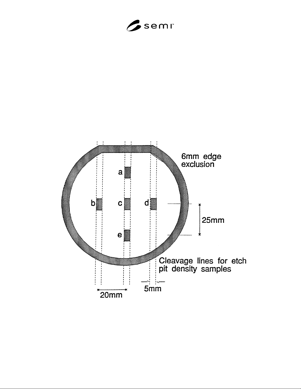
7.1.1.1 The measurement strategy is to make a detailed
measurement with an accurate fit on at least five wafer
sites, including the center as illustrated in Figure 1. The
number of wafer sites to be monitored should be agreed
on between customer and vendor. Generally, the greater
the variability relative to the mean, the larger the
number of sites that should be monitored. In each case,
the measurement system supplies a " goodness-of-fit"
parameter which indicates a level of confidence in the
fit to the measured data.
Figure 1
Schematic of Measurement Sites, Cleavage Lines, and Edge Exclusion for 100 mm SIMOX Wafer Inspection