semi合集-English.pdf - 第7477页
SEMI MF1618-1104 © SEMI 2004 7 A1-3 Concentric Circle Plans 2 A1-3.1 The concentric circle plans are designe d so that each measurement location samples approxim a tely an equal area of the specimen surface. Because thes…
SEMI MF1618-1104 © SEMI 2004 6
APPENDIX 1
SAMPLING PLANS TO BE USED FOR WAFER UNIFORMITY
DETERMINATION
NOTICE: The material in this appendix is an official part of SEMI MF1618 and was approved by full letter ballot
procedures.
A1-1 Introduction
A1-1.1 For all plans, measurements are made within a
circular area defined by the radius, R
o
, between the
center of the wafer and the circle on which the centers
of the outermost measurement sites lie. Determine this
radius by either of the following methods:
A1-1.1.1
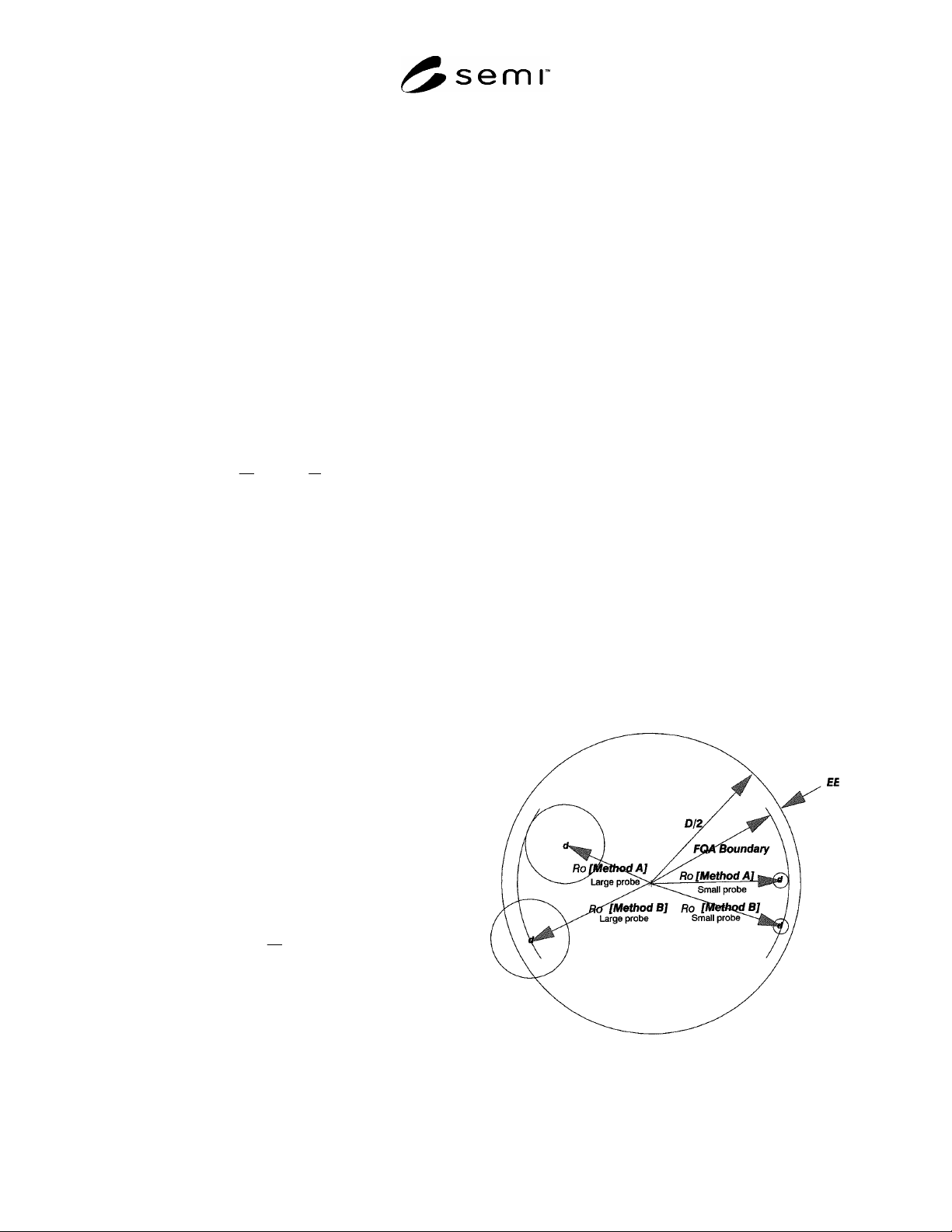
Method A — In this method, the outermost
edges of the measurement spots on the outermost radius
are tangent to the boundary of the fixed quality area
(FQA) as defined in SEMI M1:
)
2
(
2
d
EE
D
R
o
(A1-1)
where:
R
o
= radius of the outermost measurement circle (see
Figure A1-1),
D = nominal diameter of the wafer, for example,
100, 150, 200, or 300 mm,
EE = nominal wafer edge exclusion, which
determines the FQA, and
d = known or estimated diameter of the
measurement spot for the test instrument being
used (Note 1).
NOTE 1: The exact diameter of the measurement spot may
not be known for many types of measurements. Estimate the
diameter as 1.5 times the probe spacing for a four-point probe,
transducer radius for an eddy-current instrument, and apparent
beam spot radius for optical measurements if no other
information is available.
A1-1.1.2 Method B — In this method, the centers of the
measurement spots on the outermost radius are on the
boundary of the fixed quality area (FQA) as defined in
SEMI M1:
EE
D
R
o
2
(A1-2)
where the symbols are defined following Equation A1-
1.
A1-2 Selection of Method
A1-2.1 Neither of these methods is “better” than the
other; rather, there are tradeoffs.
A1-2.2
The location of every point in a multipoint
measurement pattern depends on the method chosen to
define the position of the outermost measurement sites.
Therefore, there may be differences between the two
methods for reported individual and statistical values.
A1-2.3
Data for a measurement site are usually reported
at the location corresponding with the center of the
measurement spot.
A1-2.4
Data from each measurement on the outermost
ring in Method A are not affected by the film properties
in the edge exclusion annulus outside the FQA.
However, in this case, data are not reported for
locations closer to the boundary of the FQA than the
measurement spot radius.
A1-2.5
Conversely, data from each measurement on the
outermost ring with Method B include contributions
from film properties both inside and outside the FQA.
In this case, measurement data is reported for locations
up to the boundary of the FQA, but establishing the
significance of including data influenced by film
properties outside the FQA is outside the scope of this
practice.
NOTE 2: Measurements obtained using a probe whose
effective measurement area extends beyond the edge of the
film inaccurately represent actual film properties.
Figure A1-1
FQA Boundary and Outermost Ring Radii, R
o
, for
Methods A and B
SEMI MF1618-1104 © SEMI 2004 7
A1-3 Concentric Circle Plans
2
A1-3.1 The concentric circle plans are designed so that
each measurement location samples approximately an
equal area of the specimen surface. Because these are
circular plans on a circular wafer, ideally they give
equal representation to all portions of the wafer’s
surface. This approximation to equal-area sampling
breaks down for the outermost circle if the size of the
edge exclusion is less then half the radial separation
between the inner circles for the spacing being used. In
this case, the measurements on the outer circle
represent a smaller area of silicon than do the
measurements on the inner circles. Moreover, if the
actual sampling area of the measurement being used is
larger than the value estimated in Section A1-1.1.1,
measurements on the outer circle may be partially
influenced by thin film properties in the excluded
region even though the resulting values are attributed to
the fixed quality area of the film.
A1-3.2
The concentric circle sampling plans utilize a
measurement at the wafer center and points on a
number of concentric circles designated 1, 2, 3, ... n, the
number of circles being chosen by the user according to
wafer diameter, estimated sampling area for the
measurement being made, and the amount of
information desired about the uniformity of the thin
film.
A1-3.2.1
On each circle, the measurements are
separated by equal angular intervals. Eight
measurements are made on the first circle, 16 are made
on the second circle, etc. In general, the number of
measurements is eight times the circle number. For the
first circle, measurements are separated by rotations of
45°, for the second circle, by 22.5°, and so forth,
regardless of the radial value of the measurement or the
wafer diameter.
A1-3.2.2
The radial values for the concentric circles are
determined as follows. Inspect Table A1-1 for the
number of total measurements that are made as a
function of the number of circles used and decide on the
number of circles according to the amount of
information needed for the film uniformity and the time
required for the test instrument to take that many
measurements. Call the chosen number of circles, N
C
.
Divide the value of the outermost radius, R
o
,
determined in Section A1-1.1, by N
C
. This gives the
radial increment between the circles. The center of the
measurement tool or measurement spot is to be placed
at the location given by this radial increment value.
2 Keenan, W. A., Johnson, W. M., and Smith, A. K., “Production
Monitoring of 200 mm Wafer Processing” in Emerging
Semiconductor Technology, ASTM International STP 960, edited by
D. C. Gupta and P. H. Langer (ASTM International, West
Conshohocken, PA, 1986) pp. 598–614.
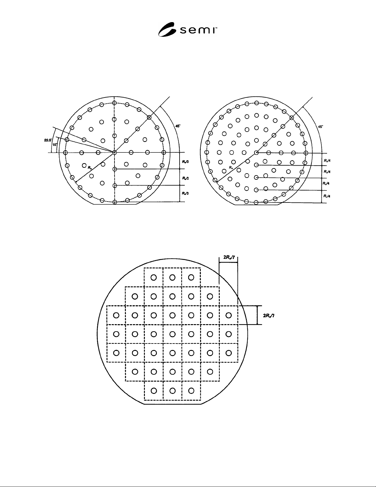
Figure A1-2 illustrates measurement locations for three-
circle and four-circle sampling plans.
NOTE 3: If the incursion of the orientation flat(s) precludes
taking valid measurements near the flat in conjunction with
the chosen edge exclusion, the parties to the test may choose
to exclude specified measurement locations if the test
instrument permits or to replace specified sites with sites at a
distance from the flat that is equal to the distance specified
with respect to the circular perimeter of the wafer. It must be
remembered, however, that either such choice may have an
adverse impact on the interpretation of any two-dimensional
contour map.
Table A1-1 Number of Measurement Sites for
Various Numbers of Concentric Circles
Number of
circles
3 4 5 6 7 8
Number of
sites
49 81 121 169 225 289
A1-3.2.3 For consistency, place the wafer on the
instrument stage with the primary flat, or notch, facing
the operator. If another convention becomes necessary,
so note it on the report. Measurements are made
starting at the center of the wafer then proceeding
around the first, then the second, then the third circle,
and so forth. For all circles, make sure that the first
measurement is made at the same angular orientation;
the positive x-axis or the positive y-axis, as defined in
the wafer coordinate system specified in SEMI M20, is
recommended. The choice should have no bearing on
the data or its analysis. However, if data is to be
presented as a time-series plot, note on the plot the
position of the first point on each circle as well as
whether the measurements proceed in a clockwise or
counterclockwise fashion on the wafer surface.
A1-3.3
Calculate the uniformity based on the difference
between the maximum and minimum measured values,
HLV(%), and on the standard deviation as a percent of
the mean of all measurements, SUP(%) as detailed in
Section 9.3.
A1-4 Cartesian Sampling Plans
A1-4.1 Cartesian sampling plans sample equal areas in
the interior of the wafer surface, but fail to sample
portions of the wafer near its perimeter. They may not
provide sufficient information about the outermost
portion of the fixed quality area for a given application.
See Figure A1-3 for an illustration in the case of a 37-
point Cartesian sampling plan.
A1-4.2
These plans have a grid of equal-sized cells,
equally spaced about the center of the wafer. A
measurement is made in the center of each cell. The
number of rows and columns in the grid, always an odd
number, is chosen according to wafer diameter,
estimated sampling area for the measurement being
SEMI MF1618-1104 © SEMI 2004 8
made, and the amount of information desired about the uniformity of the thin film. The square cells in this plan are
not necessarily the shape or size of the sampling area for the measurement being used. In general, make sure that
the sampling area for the measurement is smaller than the dimensions of the square.
(a) Three-circle Case (b) Four-circle Case
NOTE: The radius R
o
is given by Equation A1-1 for Method A and by Equation A1-2 for Method B.
Figure A1-2
Illustrations of Concentric Circle Sampling Plans
NOTE: The radius R
o
as discussed in A1-1.1 is not shown in this figure.
Figure A1-3
Illustration of the Cartesian Measurement Site Plan for the Case of Seven Rows by Seven Columns