semi合集-English.pdf - 第7483页
SEMI MF1630-0704 © SEMI 2004 3 6.5 The areas of the absorption ba nds are m easured. 6.6 Concentrations of each im purity/dopant are calculated in accordance with Bouguer-Beer’s Law with factors given in thi s test me th…

SEMI MF1630-0704 © SEMI 2004 2
3.5 Multiple internal reflections can produce a
secondary interferogram and baseline oscillations.
Changing the sample specimen thickness, the surface
preparation, or the resolution can eliminate the
secondary interferogram and the baseline oscillation.
3.6 High antimony levels interfere with the 320 cm
−1
boron absorption line. Antimony' s strongest absorption
line is 293 cm
−1
, but a secondary absorption line occurs
at 320 cm
−1
.
4 Referenced Standards
4.1 SEMI Standards
SEMI MF723 — Practice for Conversion Between
Resistivity and Dopant Density for Boron-Doped,
Phosphorus-Doped, and Arsenic-Doped Silicon
SEMI MF1241 — Terminology of Semiconductor
Technology
SEMI MF1391 — Test Method for Substitutional
Atomic Carbon Content of Silicon by Infrared
Absorption
SEMI MF1723 — Practice for Evaluation of
Polycrystalline Silicon Rods by Float-Zone Crystal
Growth and Spectroscopy
4.2 ASTM Standards
E 131 — Terminology Relating to Molecular
Spectroscopy
2
E 168 Practices for General Techniques of Infrared
Quantitative Analysis
2
E 177 — Practices for Use of the Terms Precision and
Bias in ASTM Test Methods
3
E 275 — Practice for Describing and Measuring the
Performance of Ultraviolet, Visible, and Near-Infrared
Spectrophotometers
2
NOTICE: Unless otherwise indicated, all documents
cited shall be the latest published versions.
5 Terminology
5.1 General definitions for terms related to infrared
absorption spectroscopy are found in ASTM
Terminology E 131.
5.2 Definitions for terms related to silicon materials
technology are found in SEMI MF1241.
2 Annual Book of ASTM Standards, Vol 03.06, ASTM International,
100 Barr Harbor Drive, West Conshohocken, PA 19428. Telephone:
610-832-9500, Fax: 610-832-9555, Website:
www.astm.org
3 Annual Book of ASTM Standards, Vol 14.02.
5.3 Abbreviations and Acronyms
5.3.1 FT-IR — Fourier transform infrared
(spectrometer).
5.3.2 FWHM — full width of an absorption peak
expressed in cm
−1
at half its absorbance magnitude as
measured from the baseline.
5.3.3 LTFT-IR — low temperature, Fourier transform
infrared (spectrometer).
5.4 Definitions
5.4.1 background spectrum, n — in FT-IR instruments,
the single-beam spectrum obtained without a specimen
in the infrared light path that is usually obtained with
only nitrogen, dry air, or a vacuum in the beam.
5.4.2 baseline, n — a straight line interpolation between
points on either side of the absorption peak of the
absorbance spectrum.
5.4.3 electrically active elements, n — dopants or impu-
rities in silicon that are members of either Group III
(boron, aluminum, gallium, and indium) or Group V
(phosphorus, arsenic, antimony, and bismuth) of the
periodic table.
5.4.4 sample spectrum, n — the ratio of a spectrum
obtained with the test specimen in the IR beam to a
background spectrum.
6 Summary of Test Method
6.1 A sample specimen of single crystal silicon is
cooled to less than 15 K. Under these conditions the
number of free carriers becomes negligibly small and
the IR spectrum of the sample exhibits a series of
absorption bands that are characteristic for each shallow
impurity species.
4
6.2 The sample specimen is illuminated with an
incident white light source to flood the silicon with
photons of greater energy than the silicon band gap to
allow neutralization of compensated impurities.
5
6.3 An infrared beam is directed through the sample
specimen and a transmitted spectrum is collected. The
spectrum is ratioed to the background spectrum and
then converted to an absorbance spectrum.
6.4 Baselines are constructed at one of the characteristic
absorption bands for each impurity/dopant to be
measured.
4 Kolbesen, B. O., “Simultaneous Determination of the Total
Content of Boron and Phosphorus in High-Resistivity Silicon by IR
Spectroscopy at Low Temperature,” Appl. Phys . Lett. 27, 353–355
(1975).
5 Baber, S. C., “Net and Total Shallow Impurity Analysis of Silicon
by Low Temperature Fourier Transform Infrared Spectroscopy,” Thin
Solid Films 72, 201–210 (1980).
SEMI MF1630-0704 © SEMI 2004 3
6.5 The areas of the absorption bands are measured.
6.6 Concentrations of each impurity/dopant are
calculated in accordance with Bouguer-Beer’s Law
with factors given in this test method.
7 Apparatus and Materials
7.1 Cryostat — To maintain the sample specimen
temperature below 15 K. This cryostat may be liquid
helium immersion, exchange gas, or closed cycle
refrigeration.
7.2 Sample Specimen Holder — Constructed of high
heat conductivity metal with an aperture(s) to block any
of the infrared beam except that passing through the
sample.
NOTE 1: The procedure of Section 11 is based on the
assumption that the cryostat can accommodate and utilizes a
multi-sample holder.
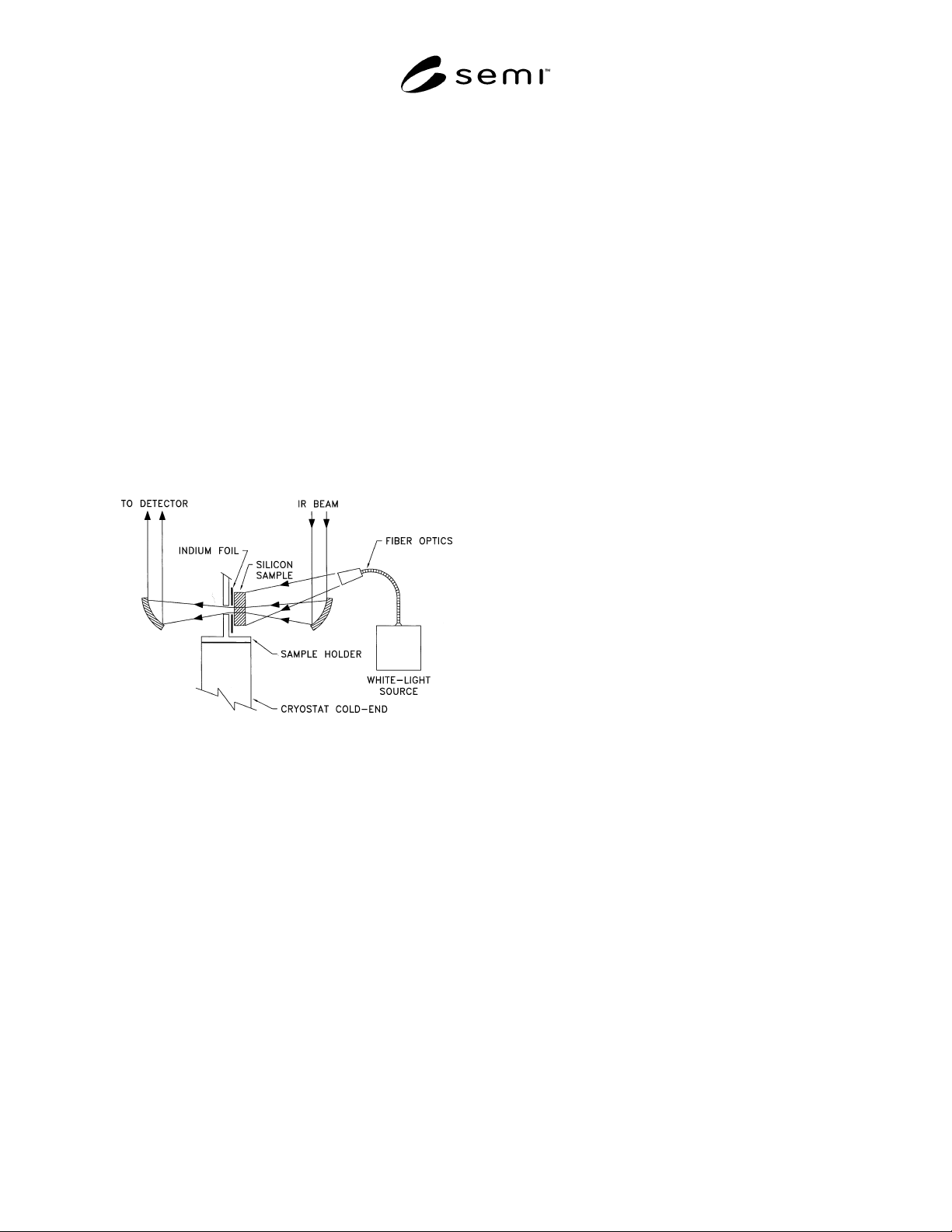
7.3 White-light Source — As shown in Figure 1.
Figure 1
Sample Holder and Optics Suitable for Illumination
with White Light via Fiber Optics
7.4 Fourier Transform Infrared Spectrometer (FT-IR)
— Must be equipped with suitable optics and detector
for use in the region from 250 cm
−1
to 1300 cm
−1
.
7.4.1 The spectrometer shall be capable of at least 1.0
cm
−1
resolution. The resolution shall be sufficient so
that after zero-filling, apodization, and Fourier
transformation the phosphorus adsorption band at 315.9
cm
−1
has a FWHM not to exceed 1.1 cm
−1
.
7.4.2 The detector shall be sufficiently sensitive to
provide a reasonable signal to noise response in the
desired spectral region. A room temperature DTGS
with a CsI window suffices for the higher
concentrations of elements in this test method.
However, a zinc-doped germanium Ge:Zn detector
operated at 4.4 to 10.0 K is preferred to give a signal-
to-noise ratio sufficient to properly determine the
elements at the lower concentrations and for improved
precision.
7.5 Calcium Fluoride Crystal (CaF
2
) — Cut to nominal
thickness of 5 mm.
8 Sample Preparation
8.1 If the samples are from polysilicon, they must first
be converted to single crystal in accordance with SEMI
MF1723 or other established means.
8.2 Sample specimen shall be cut and polished to fit the
sample specimen holder. The surface may be
mechanically or chemically polished. Each sample
specimen shall have a thickness variation of less than
1% of overall thickness.
8.3 For measurement of electrically active impurities,
the sample specimen thickness should be as follows:
8.3.1 For high purity silicon (>2000 Ω·cm): 3 to 5 mm
to allow for lower detection limits.
8.3.2 Between 5 and 20 mm in cases where impurity
levels to be measured are below 0.01 ppba.
8.3.3 For heavily doped silicon (<10 Ω·cm): 1 to 2 mm
to allow greater transmission of the infrared radiation.
9 Reference Specimens
9.1 One or more silicon samples that contain impurities
in the range of the samples to be tested shall be
classified as reference specimens. These reference
specimens should be analyzed repeatedly and
periodically according to this test method. Compare the
results obtained to previous data to establish that the
measurement process is in control.
10 Testing of the Instrument
10.1 Establish FT-IR instrument stability by checking
the 100% transmittance line.
10.1.1 Collect and store two background spectra
sequentially through an open aperture of the cryostat
specimen holder.
10.1.2 Ratio these two spectrum to obtain a
transmittance spectrum.
10.1.3 Examine the spectrum from 1200 cm
−1
to 250
cm
−1
. The spectrum should be 100 ± 0.5% T over this
range. Proceed only if the spectrum is 100 ± 5% over
this range, otherwise correct any instrumental
instability.

SEMI MF1630-0704 © SEMI 2004 4
10.2 Check for detector linearity.
6
10.2.1 Examine one of the two single-beam (unratioed)
spectra obtained in Section 10.1.1 for nonzero response
at wavenumbers where the detector is known to have
zero response (below 200 cm
−1
for the zinc doped
germanium detector with a CsI window). The observed
response in this region should be less than 1.0% of the
maximum response over the 1200 to 250 cm
−1
region.
If not, take corrective action before proceeding.
10.2.2 Alternatively, collect a spectrum with a CaF
2
crystal wafer, 5 mm-thick, in the IR beam. Ratio this
spectrum relative to one of the background spectrum
obtained in Section 10.1.1 to obtain a transmittance
spectrum. CaF
2
is totally opaque below 800 cm
−1
. The
spectrum must give 0.0 ± 0.5% transmittance from 800
to 250 cm
−1
. If not, take corrective action before
proceeding.
11 Procedure
11.1 Measure the thicknesses to ± 0.02 mm and load all
the sample specimens to be examined onto the sample
specimen holder leaving at least one open slot. Include
a reference specimen to serve as an audit to ensure that
the entire instrument is performing correctly.
11.2 Mount them in the cryostat and cool the samples to
less than 15 K.
11.3 Set instrumental parameters to give a resolution of
1.0 cm
−1
or better.
11.4 Select the reference specimen as the first sample to
be measured.
11.5 Collect 1000 scans of an empty sample chamber
slot and use this as the background spectrum.
11.6 Move the sample specimen into position.
11.7 Turn on the incident white-light source and ensure
that the sample specimen is fully illuminated with white
light and properly aligned relative to the IR beam (see
Figure 1).
11.8 Collect a minimum of 300 scans of the sample.
11.9 Zero-fill, apodize, and transform the interferogram
into a spectrum and then ratio it to the background
spectrum.
11.10 Covert to an absorbance spectrum and use as the
sample specimen spectrum.
6 Chase, D. B., “Nonlinear Detector Response in FT-IR,” Applied
Spectroscopy 38(4), 491–494 (1984).
11.11 Store this spectrum and subsequent ones for
further manipulation and measurement of the peak
areas.
11.12 Repeat Sections 11.5 through 11.11 for each
sample specimen.
12 Data Reduction
12.1 This test procedure requires the measurement of
the areas of the absorption bands before calculation of
the concentration of each element. The absorption
bands are very sharp, especially for the Group V
elements, and therefore peak height measurements are
difficult to reproduce from instrument to instrument.
Use of peak areas greatly reduces this variability.
12.1.1 Establish baselines for each peak before
measurement of the area. Use only the area above the
established baseline in the calculations. Several
algorithms are available on various commercial FT-IR
instruments to obtain the desired baseline corrected
areas. The following is one suggested method:
12.1.1.1 Retrieve the sample absorbance spectrum
from the computer storage disk. With the wavenumber
expand commands available, zoom in on the region of
the absorption band(s) of interest. Expand until this
region is only slightly larger than the baseline limit
regions given in Table 1.
12.1.1.2 Employ the interactive baseline correction
routine to bring the spectral baseline to coincide with
the 0.0 absorbance line. Refer to Table 1 for the upper
and lower wavenumber regions for guidance in
adjusting the baseline. Expand in the absorbance scale
as necessary to improve the observation of the noise
and fine features of the spectrum in order to provide the
best placement of the baseline. Apply only linear
corrections with the fit of the straight line through the
points on both sides of the absorption peak(s). Note
that the peaks for boron and phosphorus are very close
together and thus only one baseline is obtained
surrounding both peaks. Figures 2 and 3 show spectra
before and after, respectively, baseline correction for
boron and phosphorus spectral region.
12.1.2 Measure the area for the absorption peak
between the upper and lower wavenumbers given in
Table 1 for the integration limits. Most computer
algorithms handle this nicely. However, disable the
automatic zeroing of the baseline at the integration
limits. If not disabled, the integration would not
represent the baseline as established in Section 12.1.1
and may result in errors.
12.1.3 Repeat Sections 12.1.1 and 12.1.2 for each
component desired for each specimen measured.