semi合集-English.pdf - 第5066页
SEMI M22-0303 © SEMI 1992, 2003 1 SEMI M22-0303 SPECIFICATION FOR DIELECTRICAL LY ISOLATED (DI) WAFERS This specification was technically approved by th e Global Silicon Wafer Committee and is the direct responsibility o…
SEMI M21-0304 © SEMI 1992, 2004 10
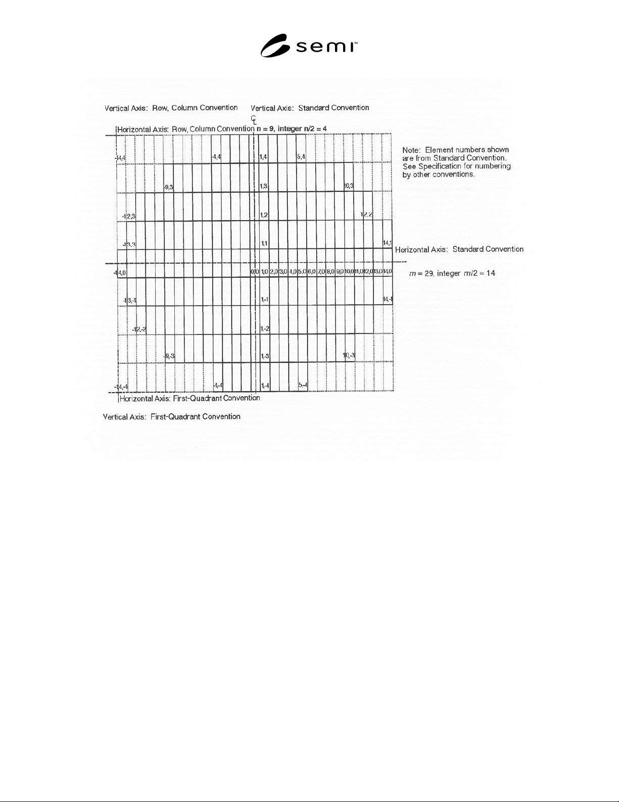
Figure R2-1
Comparison of Array Addressing Conventions
NOTICE: SEMI makes no warranties or representations as to the suitability of the standards set forth herein for any
particular application. The determination of the suitability of the standard is solely the responsibility of the user.
Users are cautioned to refer to manufacturer’s instructions, product labels, product data sheets, and other relevant
literature respecting any materials mentioned herein. These standards are subject to change without notice.
The user’s attention is called to the possibility that compliance with this standard may require use of copyrighted
material or of an invention covered by patent rights. By publication of this standard, SEMI takes no position
respecting the validity of any patent rights or copyrights asserted in connection with any item mentioned in this
standard. Users of this standard are expressly advised that determination of any such patent rights or copyrights, and
the risk of infringement of such rights, are entirely their own responsibility.
Copyright by SEMI® (Semiconductor Equipment and Materials
International), 3081 Zanker Road, San Jose, CA 95134. Reproduction o
f
the contents in whole or in part is forbidden without express written
consent of SEMI.
SEMI M22-0303 © SEMI 1992, 2003 1
SEMI M22-0303
SPECIFICATION FOR DIELECTRICALLY ISOLATED (DI) WAFERS
This specification was technically approved by the Global Silicon Wafer Committee and is the direct
responsibility of the North American Silicon Wafer Committee. Current edition approved by the North
American Regional Standards Committee on October 25, 2002. Initially available at www.semi.org
December 2002; to be published March 2003. Originally published in 1992; previously published in
December 1996.
1 Purpose
1.1 Dielectrically isolated (DI) wafers are used for
fabricating specialized semiconductor devices,
including radiation tolerant devices. This specification
is intended to aid the definition and procurement of
such wafers.
2 Scope
2.1 This specification defines requirements for DI
wafers used for semiconductor device manufacture. By
defining inspection procedures and acceptance criteria,
both suppliers and consumers may uniformly define
product characteristics and quality requirements.
NOTE 1: This document currently applies only to DI wafers
with nominal diameter of 100 mm.
2.2 The primary standardized properties set forth in
this specification relate to physical, electrical, and
surface defect parameters of DI wafers.
2.3 A complete purchase specification requires that
additional physical properties be specified along with
suitable test methods for their measurements.
NOTICE: This standard does not purport to address
safety issues, if any, associated with its use. It is the
responsibility of the users of this standard to establish
appropriate safety and health practices and determine
the applicability of regulatory or other limitations prior
to use.
3 Referenced Standards
3.1 SEMI Standard
SEMI M1 — Specifications for Polished
Monocrystalline Silicon Wafers
3.2 ASTM Standard
1
F 523 — Practice for Unaided Visual Inspection of
Polished Silicon Slices
1 American Society for Testing and Materials, 100 Barr Harbor
Drive, West Conshohocken, Pennsylvania 19428-2959, USA.
Telephone: 610.832.9585, Fax: 610.832.9555 Website:
www.astm.org
3.3 Other Standard
2
ANSI/ASQC Z1.4-1993 — Sampling Procedures and
Tables for Inspection by Attributes
NOTICE: Unless otherwise indicated, all documents
cited shall be the latest published versions.
4 Terminology
4.1 Definitions
4.1.1 concentricity — The distance between the
centerpoint of the DI wafer and the centerpoint of the
photolithographic pattern.
4.1.2 connected tubs — Adjacent tubs which are not
completely surrounded by an oxide but are connected
by silicon (see Figure 1).
4.1.3 DI wafer — A wafer consisting of polysilicon,
oxide, and single crystal silicon regions. A typical
cross-section is shown in Figure 2.
4.1.4 edge indent — An edge defect on a DI wafer that
extends from the front surface to the back surface.
4.1.5 electrical die — An identifiable repetitive
monolithic combination of tubs and polysilicon areas in
a DI wafer surrounded by a grid border which as
packaged becomes a component.
4.1.6 layer of polycrystalline silicon — The thick
matrix material of a DI wafer in which the silicon tubs
reside.
4.1.7 pattern deformation — A microscopic defect
associated with missing or indented tub features of 4
microns or more (see Figure 3).
4.1.8 rotation — The angle of deviation between the
primary flat of the DI wafer and the x-axis of the
photolithography pattern.
4.1.9 tub — A single crystal silicon region in a DI
wafer which is surrounded by an oxide layer on the
sides and bottom.
2 American National Standards Institute, New York Office: 11 West
42nd Street, New York, NY 10036, USA. Telephone: 212.642.4900;
Fax: 212.398.0023 Website: www.ansi.org
SEMI M22-0303 © SEMI 1992, 2003 2
4.1.10 tub depth — The thickness of the tub as
measured from the wafer surface to the buried oxide
layer parallel to the wafer surface (see Figure 2).
4.1.11 void in the polycrystalline silicon — A
microscopic depression on the surface of polysilicon
areas in DI wafers (see Figure 4).
5 Ordering Information
5.1 Purchase orders for dielectrically isolated wafers
shall include the following items:
5.1.1 Tub Characteristics
A. Resistivity
B. Conductivity and Dopant Type
C. Crystal Growth Method (Czochralski or Float Zone)
5.1.2 Tub Diffused Layers (if required)
A. Sheet Resistance
B. Junction Depth
C. Dopant Type
5.1.3 Polysilicon Resistivity
5.1.4 Nominal Tub Depth
5.1.5 Method of Pattern Transfer from User to Supplier
5.1.5.1 The pattern transfer of electrical die
information may be accomplished through a physical
exchange of photomasks or through a data exchange.
Issues such as corner compensations, design rules, and
alignment features shall be agreed upon between the
supplier and purchaser.
5.1.6 Oxide Thickness of Isolation Layer
5.1.7 Methods of Test and Measurements (see Section
7)
5.1.8 Lot Acceptance Procedures (see Section 8)
5.1.9 Certification (if required) (see Section 9)
5.1.10 Packing and Marking (see Section 10)
6 Requirements
6.1 The complete specification for the starting
substrates to produce DI wafers includes all general
requirements of SEMI M1.
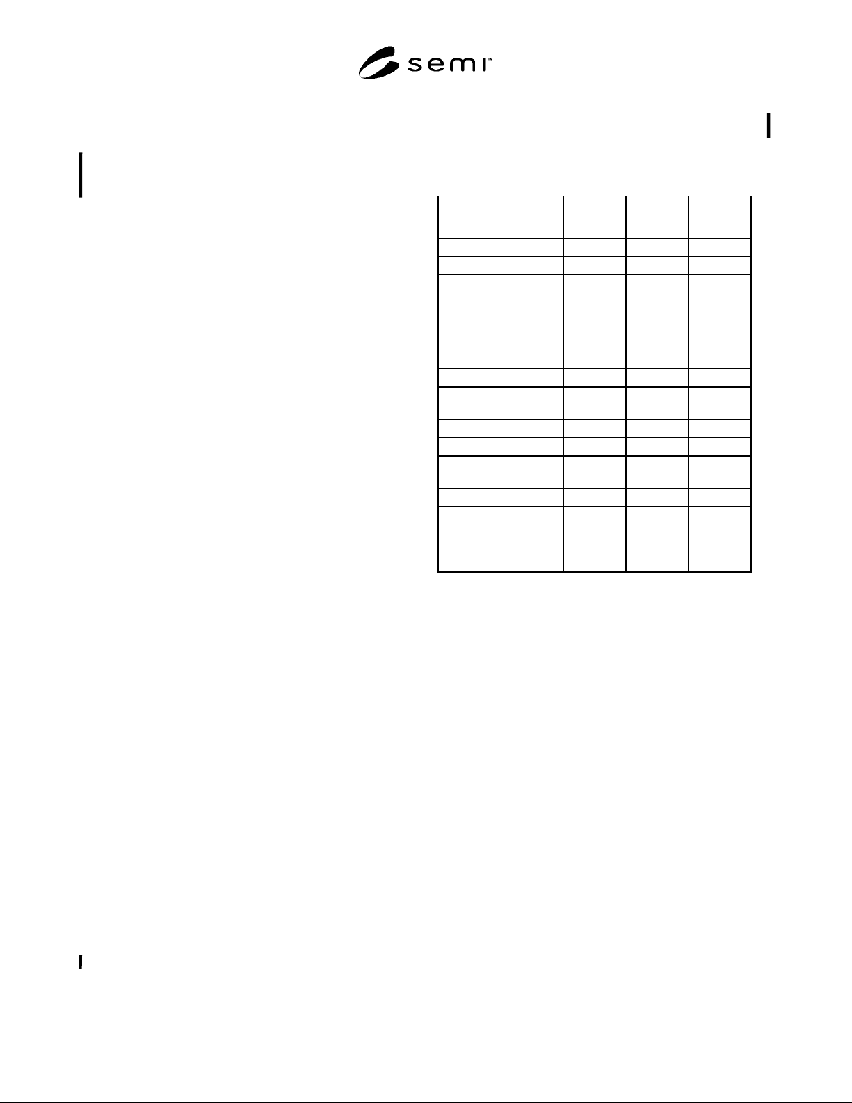
6.2 The Dimension and Tolerance Requirements for
100 mm DI wafers are listed in Table 1.
6.3 Visual defects on a wafer shall not exceed the
limits established in Table 2.
6.4 Microscopic defects on a die and defective die on a
wafer shall not exceed the limits as established in Table
3. To meet these specifications, at least 75% of the die
on a wafer must be defect free.
Table 1 Dimension and Tolerance Requirements
Property Dimension Tolerance Units (see
Note 1)
Diameter 100 ± 0.50 mm
Thickness, Center Point 508 ± 25 mm
Surface Orientation,
referenced to tub
crystal axes
{100} ± 1 deg
Primary Flat
Orientation, referenced
to tub crystal axes
{110} ± 1 deg
Primary Flat Length 32.5 ± 2.5 mm
Secondary Flat
Location, optional
Secondary Flat Length 18.0 ± 2.0 mm
Bow, Max. + 380 µm
Total Thickness
Variation, Max.
25 µm
Concentricity, Max. 3 mm
Rotation, Max. 2 deg
Edge Profile
Coordinate, C
y
(see
Note 2)
170 µm
Note 1: For referee purposes the metric (SI) units apply.
Note 2: See SEMI M1, Figure 4.