semi合集-English.pdf - 第867页
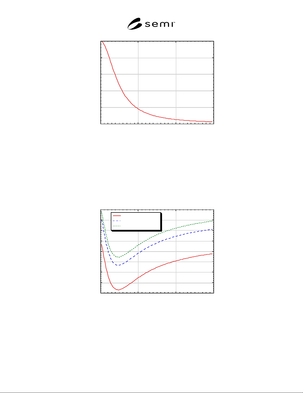
SEMI E115-0302 E © SEMI 2002 13 0.0 10.0 20.0 30.0 40.0 50.0 0 500 1000 1500 Real Impedance (ohms) C1 Capacitance (pF) NOTE 1: The real impedance varies fro m 1.2 ohms to close to 50 ohms. Figure R1-3 Example Plo t of th…
SEMI E115-0302
E
© SEMI 2002 12
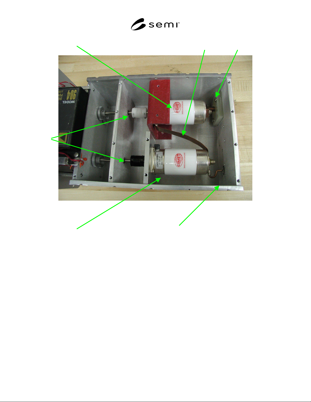
Series Capacitor Strap Input
Rotating
Shafts
Shunt Capacitor Output
NOTE 1: Picture of a Load Simulator showing the variable capacitors. The capacitors are connected together by a strap that has
an inductance of around 100 nH. The values of the capacitors are varied by rotating their shafts. The ends of the shafts are
connected to a dial indicator to measure their positions.
Figure R1-2
Picture of a Load Simulator Showing the Variable Capacitors
SEMI E115-0302
E
© SEMI 2002 13
0.0
10.0
20.0
30.0
40.0
50.0
0 500 1000 1500
Real Impedance (ohms)
C1 Capacitance (pF)
NOTE 1: The real impedance varies from 1.2 ohms to close to 50 ohms.
Figure R1-3
Example Plot of the Real Part of the Load Impedance as a Function of the C1 Shunt Capacitor in the Load
Simulator
-40.0
-35.0
-30.0
-25.0
-20.0
-15.0
-10.0
-5.0
0.0
0 500 1000 1500
C2 = 500 pF
C2 = 1000 pF
C2 = 1500 pF
Reactive Impedance (ohms)
C1 Capacitance (pF)
NOTE 1: The C2 capacitance is at the indicated fixed value for each set of data. For this example, the reactive impedance varies
from around –40 ohms to –5 ohms. Decreasing C2 to 100 pF reduces the reactance to less than –100 ohms.
Figure R1-4
Example Plot of the Reactive Part of the Load Impedance as a Function of the C1 Shunt Capacitance in the
Load Simulator
SEMI E115-0302
E
© SEMI 2002 14
RF out R
A
B
Port 2Port 1
Port 1
Port 2
Perform Calibrations
at End of Additional
Test Cables
Load Simulator
Input Connection
Output Connection
C2
C1
Network
Analyzer
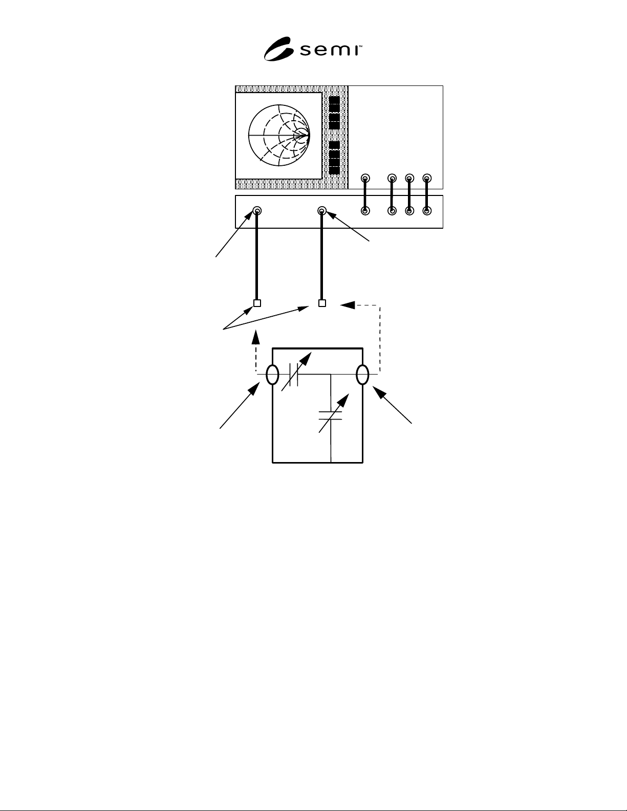
NOTE 1: Both the Port 1 and Port 2 outputs need to be used for the measurement. Additional test cables are needed for the
transmission calibration between the two ports. The input connection of the Load Simulator attaches to Port 1 of the Network
Analyzer. The output connection of Load Simulator attaches to Port 2 of the Network Analyzer.
Figure R1-5
Schematic of a Load Simulator Test Setup for the Load Impedance and Efficiency Measurement
NOTICE: SEMI makes no warranties or representations as to the suitability of the standards set forth herein for any
particular application. The determination of the suitability of the standard is solely the responsibility of the user.
Users are cautioned to refer to manufacturer' s instructions, product labels, product data sheets, and other relevant
literature, respecting any materials or equipment mentioned herein. These standards are subject to change without
notice.
By publication of this standard, Semiconductor Equipment and Materials International (SEMI) takes no position
respecting the validity of any patent rights or copyrights asserted in connection with any items mentioned in this
standard. Users of this standard are expressly advised that determination of any such patent rights or copyrights, and
the risk of infringement of such rights are entirely their own responsibility.
Copyright by SEMI® (Semiconductor Equipment and Materials
International), 3081 Zanker Road, San Jose, CA 95134. Reproduction o
f
the contents in whole or in part is forbidden, without express written
consent of SEMI.