semi合集-English.pdf - 第6509页
SEMI G80-0200 © SE MI 2000 17 Table 1 Data Collect ion Table for Levels 1 and 2 Test Numbe r Channe l Number Min. Value Max. Value Section 10.3.1 Tim ing Linea rit y Tes t (Driv e Input Edge Pl acement) m to n Section 10…
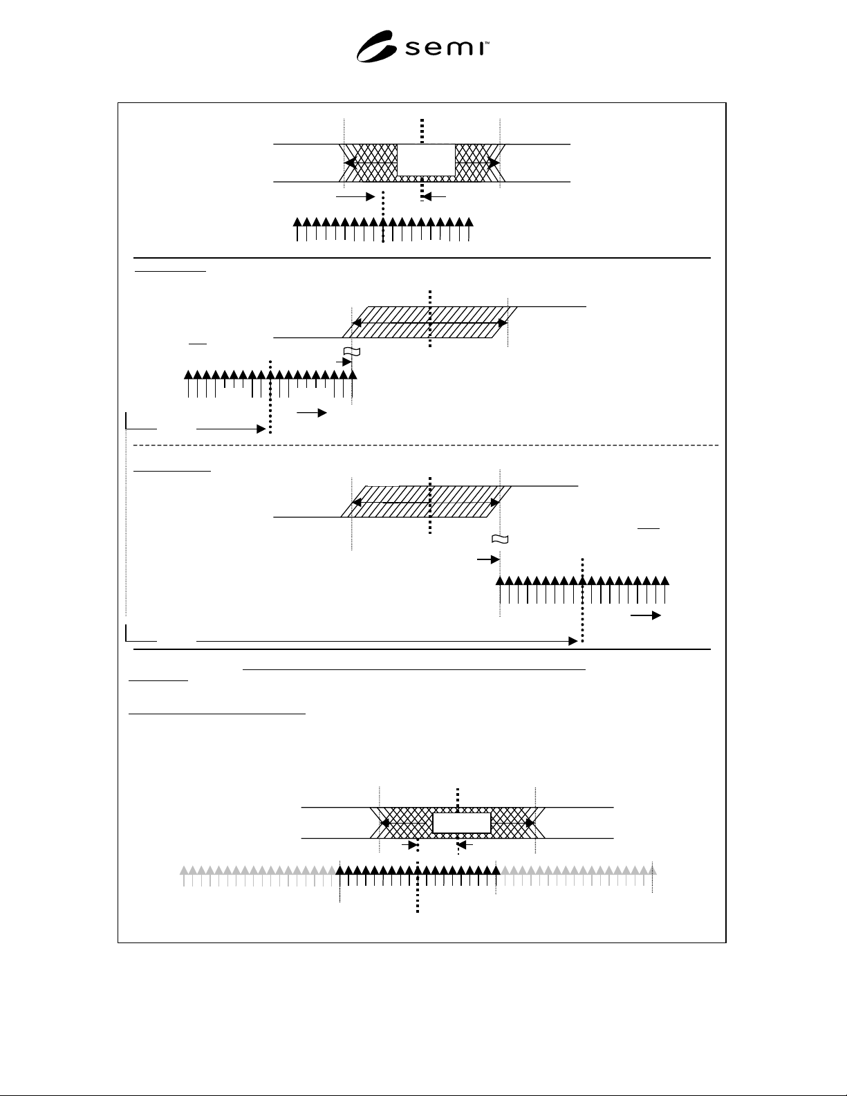
SEMI G80-0200 © SEMI 2000 16
Compare Error
MIN Value- MIN is the value all
comparators are programmed to
when the first drive edge is
detected.
For a sweep- Compare edges
should be programmed far in
advance of the reference
signal allowing enough room
to detect the earliest
occurrence of a drive ed
g
e.
TIMING RELATIONSHIPS, DEFINITIONS & EXAMPLE RESULTS
DEFINITIONS-
Reference- The programmed value of the drivers
Drive to Compare Error- The difference between the average of min & max for Drive and the
average of min & max for Compare error.
RELATIONSHIPS & EXAMPLE RESULTS-
Negative Error: Reference - Min Value = 1000ps - 850ps = 150ps
Positive Error: Reference - Max Value = 1000ps - 1250ps = -250ps
Drive to Compare Error: Reference - [(Min Value + Max Value)/2] = 1000ps - [(850ps + 1250ps)/2] = -50ps
For a sweep- Compare edges
should be programmed fa
r
b
eyond the reference signal
allowing enough room to detec
t
the latest occurrence of a drive
d
MAX drive value- Detect the
latest occurrence of the drive edge
with the earliest compare edge
(last fail- Timing Linearity Test
10.3.1)
MIN drive value- Detect the
earliest occurrence of the drive
edge with the latest compare
edge (first pass- Timing
Linearity Test 10.3.1)
-100ps
Drive Edges
1000ps Drive
Reference
+100ps
-100
p
s +100
p
s
Drive Error
Drive
Reference
-100ps +100ps
Drive Edges
In this example:
Drive edge error = ±100ps
Compare edge error = ±100ps
Drive to Compare error = - 50ps
This example will illustrate how
numerical error values are
obtained.
Max Value- MAX is the value
all comparators are programmed
to when the last drive edge is
detected.
-100ps
1000ps
Drive
+100ps
N
OTE: All drive edges are
detected in parallel in pairs:
pin 1 & 2, 3 & 4,...n-1 & n.
N
OTE: All drive edges are
detected in parallel in pairs: pin 1
& 2, 3 & 4,...n-1 & n.
850
p
s
1050ps
950ps
1000ps Reference
-100
p
s +100
p
s
50
p
s
Drive
Reference
-100ps +100ps
First Pass
Min Value
Last Fail
Max Value
When the edges on all pins are
detected the drive to compare
error relationship will appear as
indicated here with associate
d
error values indicated.
1250ps
(Max value)
Sweep
Last fail
850ps
(Min value)
SweepCompare Edges
First pass
0ns
850ps
+100ps-100ps
+900ps
0ns
1250ps
Compare Edges
+100ps-100ps
1250ps
50ps
N
OTE: Additional information
related to this figure is contained
in Appendix 2.
Drive to Compare Edge Error
Figure 7
Level 1 Drive Edge Error = Compare Error
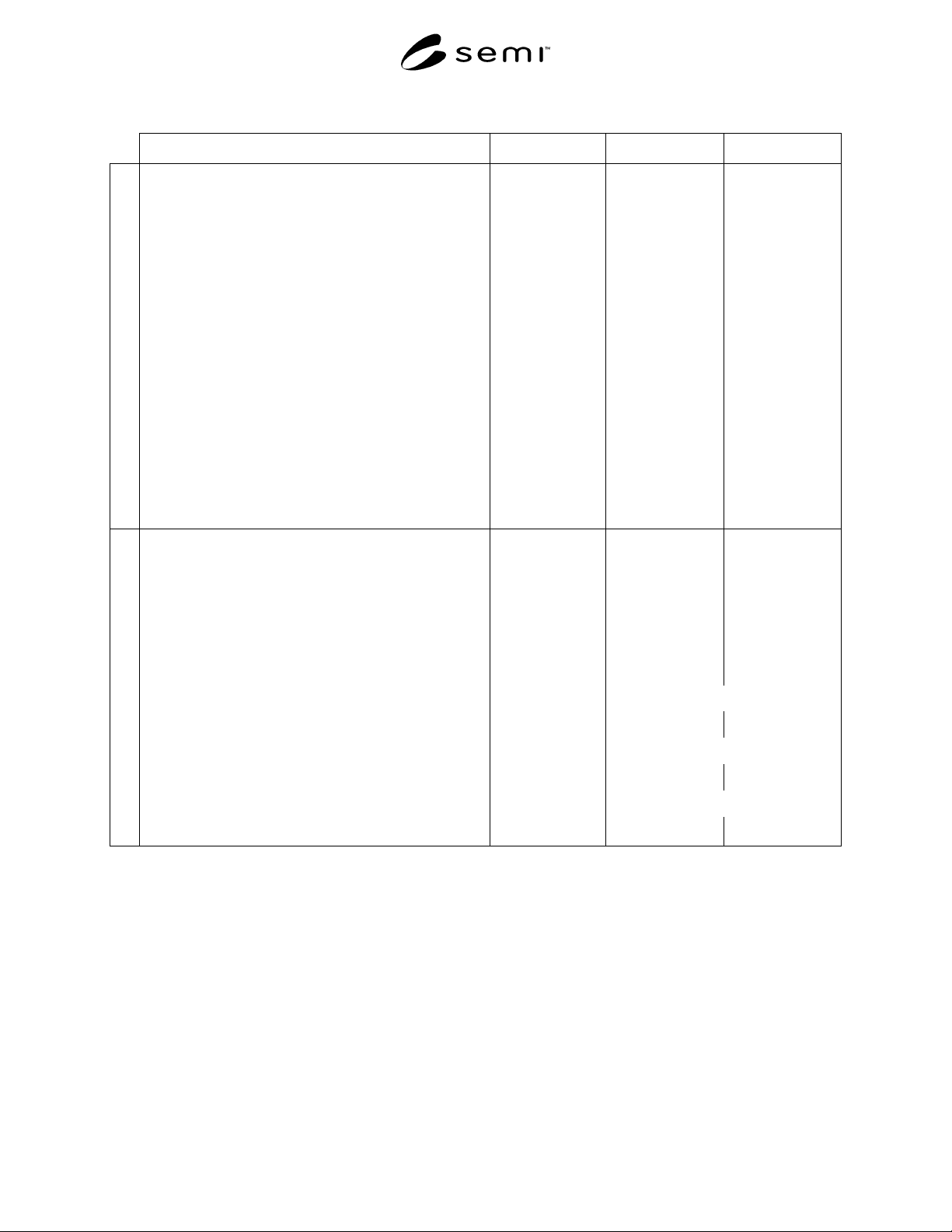
SEMI G80-0200 © SEMI 200017
Table 1 Data Collection Table for Levels 1 and 2
Test Number Channel Number Min. Value Max. Value
Section 10.3.1 Timing Linearity Test
(Drive Input Edge Placement)
m
to
n
Section 10.3.4 Extended Delay Test
(Compare Output Edge Placement)
m
to
n
Section 10.3.5 Drive Input Z Timing Error
(Z to 0 (Low))
m
to
n
Section 10.3.5 Drive Input Z Timing Error
(Z to 1 (High))
m
to
n
Section 10.3.5 Drive Input Z Timing Error
(0 (Low) to Z)
m
to
n
Section 10.3.5 Drive Input Z Timing Error
(1 (High) to Z)
m
to
n
L
E
V
E
L
O
N
E
Section 10.3.6 Multiple Period Test
(Optional- for on the fly timing)
m
to
n
Section 10.4.1 Drive Input Time Delay Error
(Drive Input Edge Placement)
m
to
n
Section 10.4.2 Compare Output Time Delay Error
(Compare Output Edge Placement)
m
to
n
Section 10.4.3 Drive Input Transition Time Variation m
to
n
Enter RMS value onlySection 10.4.4 Drive Input Timing Cycle Jitter
(Short term cycle to cycle period jitter)
m
to
n
Enter RMS value onlySection 10.4.5 High Speed Clock Self Trigger Cycle Jitter
(Short term cycle to cycle period jitter/clocks)
m
to
n
Enter RMS value only
L
E
V
E
L
T
W
O
Section 10.4.6 High Speed Clock Self Trigger Phase Jitter
(Short term phase /duty cycle jitter/clocks)
m
to
n
NOTE 6: This is a generic example of the data table needed to gather the data values for this timing analysis procedure. The
actual number of table entries will depend upon the number of tester pins under evaluation. The pins to be tested are represented
by the designation “m” to “n”. For Level 1 the application program is expected to fill in the minimum and maximum
measurements made for each pin and specified condition. For Level 2 the user will fill-in these data values via manual entry,
unless the application and implementation method employ automated/robotic operation.
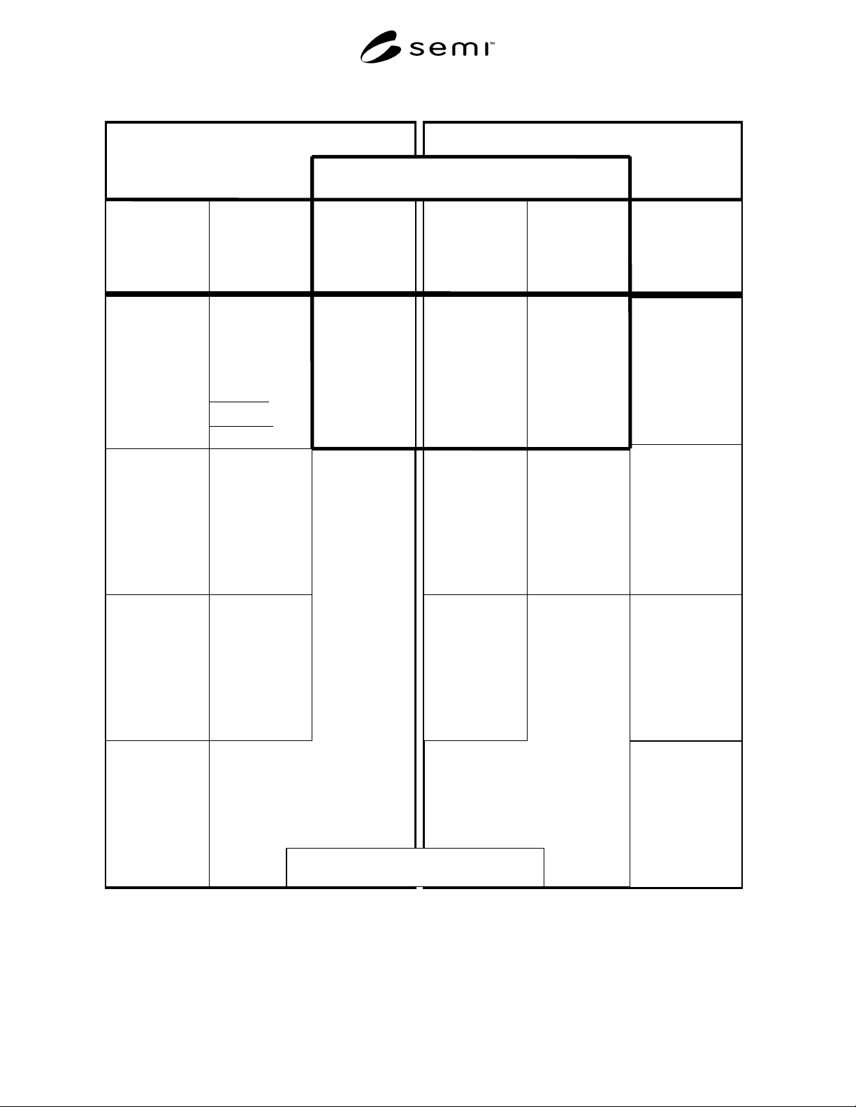
SEMI G80-0200 © SEMI 2000 18
Table 2 Test Method Summary Table for Establishing Overall Timing Accuracy (OTA)
LEVEL 1
Timing Linearity
Extended Delay
Multiple Period
Data below represents
Level 1edge-delay results
LEVEL 2
High Speed Clock
Accuracy
Data to enter here =
"a" below:
Drive Input Z
Timing Error Level
1 (Section 10.3.5) Z
to 0 (Low)-
Data to enter here is
Positive Error and
Negative Error per
the data in Table 1
and Equation 1
Appendix 2.
Timing Linearity
Level 1 (Sec.10.3.1)
Data to enter here is
Positive Error &
Negative Error per
the data in Table 1
and the 2 equations:
Positive Error =
Reference - Max Value
N
egative Error =
Reference -Min Value
d) High Speed Clock
Self Trigger Phase
Jitter Level 2 (Section
10.4.6)-
Data to enter here =
the RMS value in
Table 1.
c) High Speed Clock
Self Trigger
Cycle Jitter Level 2
(Section 10.4.5)
Data to enter here =
the RMS value in
Table 1.
Extended Delay
Level 1 (Sec.
10.3.4)- Data to
enter here is
Positive Error and
Negative Error per
the data in Table 1
and Equation 1
Appendix 2.
Multiple Period
Level 1 Optional
(Sec. 10.3.6) Data
to enter here is
Positive Error and
Negative Error per
the data in Table 1
and Equation 1
Appendix 2.
Drive Input Z
Timing Error Level
1 (Section 10.3.5) Z
to 1 (High)-
Data to enter here is
Positive Error and
Negative Error per
the data in Table 1
and Equation 1
Appendix 2.
Drive Input Z
Timing Error Level
1 (Section 10.3.5) 0
(Low) to Z -
Data to enter here is
Positive Error and
Negative Error per
the data in Table 1
and Equation 1
Appendix 2.
Drive Input Z
Timing Error Level
1 (Section 10.3.5) 1
(High) to Z-
Data to enter here is
Positive Error and
Negative Error per
the data in Table 1
and Equation 1
Appendix 2.
1) Drive Input To
Compare Output
Timing
Data to enter here is
Drive Input to Compare
Output (value below)
3) Compare Output
Edge Placement
Data to enter here = a)
Compare Output Time
Delay Error
2) Drive
Input Edge
Placement
Data to enter here =
"a" below:
Drive Input to
Compare Out put
Timing Accuracy
calculated from
10.3.1 data as:
Reference -
[(MinValue+Max
Value)/2]. Refer to
examples in
Appendix 2.
a) Compare Output
Time Delay Error
Level 2 (Section
10.4.2) Data to
enter here = the
delta between the
min and max values
in Table 1.
a) Drive Input
Timing Delay Error
Level 2 (Section
10.4.1)-
Data to enter here =
the delta between
the min and max
values in Table 1.
b) Drive Input
Transition Time
Variation
Level 2 (Section
10.4.3) -
Data to enter here =
the delta between
the min and max
values in Table 1.
b) Compare Output
Timing Jitter
(Note: no method
exists for this test)
c) Drive Input
Timing Cycle Jitter
Level 2 (Section
10.4.4)
Data to enter here =
the RMS value in
Table 1.
Single Point Overall Timing Accuracy (OTA) Results
Data to enter here is: A = Dr (item 2) + Cmp (item 3) + Dr-Cmp (item 1)
-B = -Dr (item 2) - Cmp (item 3) + Dr-Cmp (item 1)
.
Drive Z Timing
Data below represents
Level 1 Z- state timing
results
a) High Speed Clock
Delay Error (Section
10.4.1- same as Drive
Input Timing Delay
but for clock pins)
Data taken and
entered for these pins
equivalent to Drive
Input Timing
b) High Speed Clock
Transition time
variation (Section
10.4.3- same as drive
input transition time
but for clock pins)
Data entry equivalent
to Drive Input
Transition Time.
The user of the method is advised to read Section
13, Precautions before filling in this table.