semi合集-English.pdf - 第6183页
SEMI G38-0996 © SEMI 1987, 2004 8 APPENDIX 1 REPORT FORMAT NOTICE : This ap pendix was approved as a n official part of SEMI G38 by f ull letter ba llot procedure. The following format is a sample of report format: 1. De…
SEMI G38-0996 © SEMI 1987, 2004 7
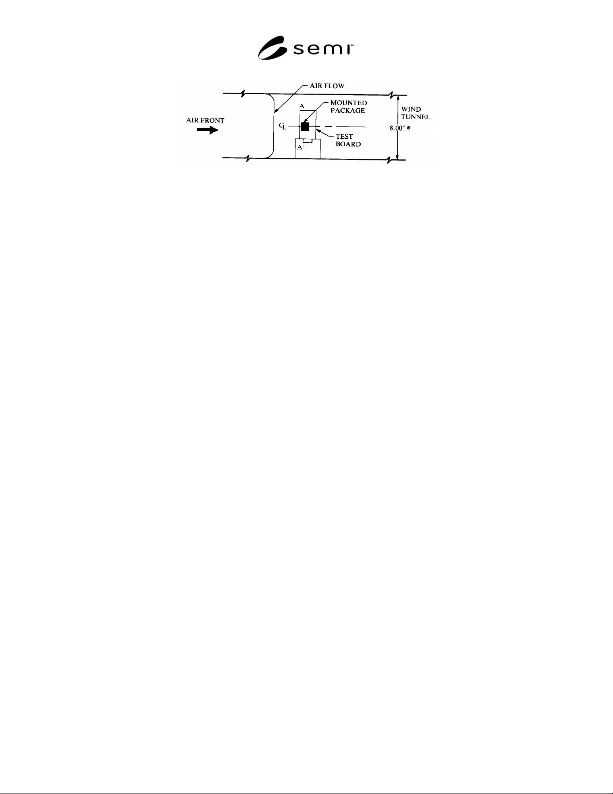
Figure 3
Test Board Orientation Inside Wind Tunnel

SEMI G38-0996 © SEMI 1987, 2004 8
APPENDIX 1
REPORT FORMAT
NOTICE: This appendix was approved as an official part of SEMI G38 by full letter ballot procedure.
The following format is a sample of report format:
1. Description of Package
1.1 Package Type
Package Name ________________ (per JEDEC or EIAJ)
Pin Counts ________________ pins
Special Specification ________________ Yes ________________ No
1.2 Test Chip
Chip per SEMI G32 ________________ Yes ________________ No
Chip Size ________________ mm x ________________ mm
Chip Thickness ________________ mm
1.3 Leadframe
Leadframe Material Fe/Ni Alloy, Cu, Cu Alloy, Other (________________)
Leadframe Thickness ________________ mm
Die Pad Size ________________ mm x ________________ mm
1.4 Package Dimension & Compound
Package Size ________________ mm x ________________ mm
Package Thickness ________________ mm
Compound Material ________________________________
1.5 Others
Die Attach Material ________________________________
Heat Sink/Spreader ________________ Yes ________________ No
2. Description of Test Board
Test Board per SEMI G42 ________________ Yes ________________ No
No. of Layers ________________________________
3. Measurement Result
Power Dissipation ________________ W
SEMI G38-0996 © SEMI 1987, 2004 9
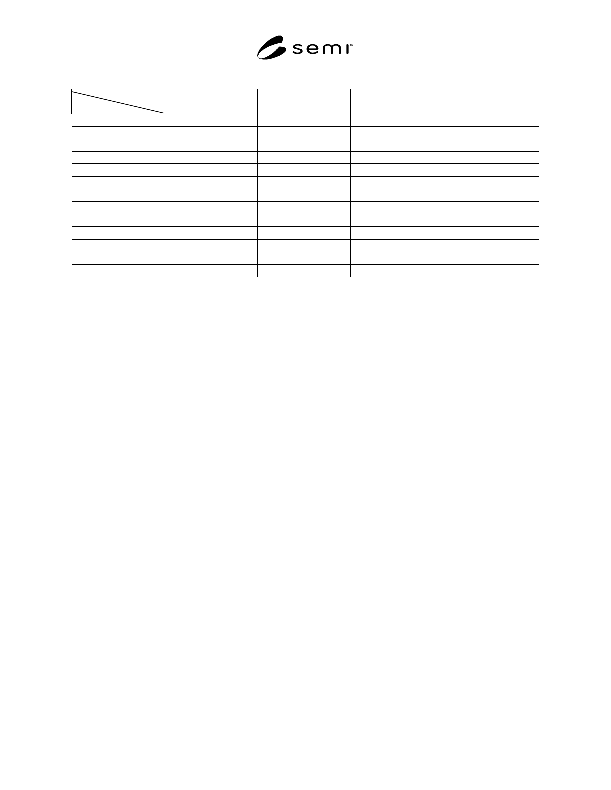
Units: °C/W
Air Velocity (m/s)
Sample No.
0 1 3 5
1
2
3
4
5
6
7
8
9
10
Average
NOTICE: SEMI makes no warranties or representations as to the suitability of the standards set forth herein for any
particular application. The determination of the suitability of the standard is solely the responsibility of the user.
Users are cautioned to refer to manufacturer’s instructions, product labels, product data sheets, and other relevant
literature respecting any materials mentioned herein. These standards are subject to change without notice.
The user’s attention is called to the possibility that compliance with this standard may require use of copyrighted
material or of an invention covered by patent rights. By publication of this standard, SEMI takes no position
respecting the validity of any patent rights or copyrights asserted in connection with any item mentioned in this
standard. Users of this standard are expressly advised that determination of any such patent rights or copyrights, and
the risk of infringement of such rights, are entirely their own responsibility.
Copyright by SEMI® (Semiconductor Equipment and Materials
International), 3081 Zanker Road, San Jose, CA 95134. Reproduction o
f
the contents in whole or in part is forbidden without express written
consent of SEMI.