semi合集-English.pdf - 第7485页
SEMI MF1630-0704 © SEMI 2004 5 Table 1 Peak Location, Baseline an d Integration Limits, and Calibration Facto rs Baseline Limits Integration Limits Element Peak cm − 1 Upper Lower Upper Lower Factor A f(mm-cm) Aluminum (…

SEMI MF1630-0704 © SEMI 2004 4
10.2 Check for detector linearity.
6
10.2.1 Examine one of the two single-beam (unratioed)
spectra obtained in Section 10.1.1 for nonzero response
at wavenumbers where the detector is known to have
zero response (below 200 cm
−1
for the zinc doped
germanium detector with a CsI window). The observed
response in this region should be less than 1.0% of the
maximum response over the 1200 to 250 cm
−1
region.
If not, take corrective action before proceeding.
10.2.2 Alternatively, collect a spectrum with a CaF
2
crystal wafer, 5 mm-thick, in the IR beam. Ratio this
spectrum relative to one of the background spectrum
obtained in Section 10.1.1 to obtain a transmittance
spectrum. CaF
2
is totally opaque below 800 cm
−1
. The
spectrum must give 0.0 ± 0.5% transmittance from 800
to 250 cm
−1
. If not, take corrective action before
proceeding.
11 Procedure
11.1 Measure the thicknesses to ± 0.02 mm and load all
the sample specimens to be examined onto the sample
specimen holder leaving at least one open slot. Include
a reference specimen to serve as an audit to ensure that
the entire instrument is performing correctly.
11.2 Mount them in the cryostat and cool the samples to
less than 15 K.
11.3 Set instrumental parameters to give a resolution of
1.0 cm
−1
or better.
11.4 Select the reference specimen as the first sample to
be measured.
11.5 Collect 1000 scans of an empty sample chamber
slot and use this as the background spectrum.
11.6 Move the sample specimen into position.
11.7 Turn on the incident white-light source and ensure
that the sample specimen is fully illuminated with white
light and properly aligned relative to the IR beam (see
Figure 1).
11.8 Collect a minimum of 300 scans of the sample.
11.9 Zero-fill, apodize, and transform the interferogram
into a spectrum and then ratio it to the background
spectrum.
11.10 Covert to an absorbance spectrum and use as the
sample specimen spectrum.
6 Chase, D. B., “Nonlinear Detector Response in FT-IR,” Applied
Spectroscopy 38(4), 491–494 (1984).
11.11 Store this spectrum and subsequent ones for
further manipulation and measurement of the peak
areas.
11.12 Repeat Sections 11.5 through 11.11 for each
sample specimen.
12 Data Reduction
12.1 This test procedure requires the measurement of
the areas of the absorption bands before calculation of
the concentration of each element. The absorption
bands are very sharp, especially for the Group V
elements, and therefore peak height measurements are
difficult to reproduce from instrument to instrument.
Use of peak areas greatly reduces this variability.
12.1.1 Establish baselines for each peak before
measurement of the area. Use only the area above the
established baseline in the calculations. Several
algorithms are available on various commercial FT-IR
instruments to obtain the desired baseline corrected
areas. The following is one suggested method:
12.1.1.1 Retrieve the sample absorbance spectrum
from the computer storage disk. With the wavenumber
expand commands available, zoom in on the region of
the absorption band(s) of interest. Expand until this
region is only slightly larger than the baseline limit
regions given in Table 1.
12.1.1.2 Employ the interactive baseline correction
routine to bring the spectral baseline to coincide with
the 0.0 absorbance line. Refer to Table 1 for the upper
and lower wavenumber regions for guidance in
adjusting the baseline. Expand in the absorbance scale
as necessary to improve the observation of the noise
and fine features of the spectrum in order to provide the
best placement of the baseline. Apply only linear
corrections with the fit of the straight line through the
points on both sides of the absorption peak(s). Note
that the peaks for boron and phosphorus are very close
together and thus only one baseline is obtained
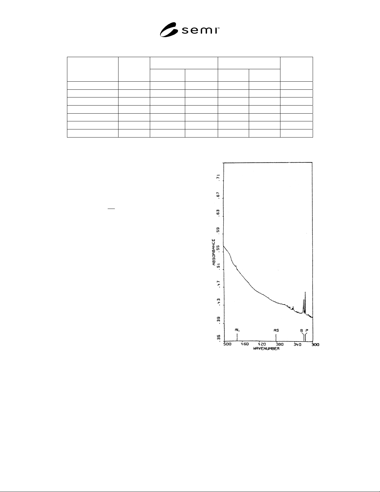
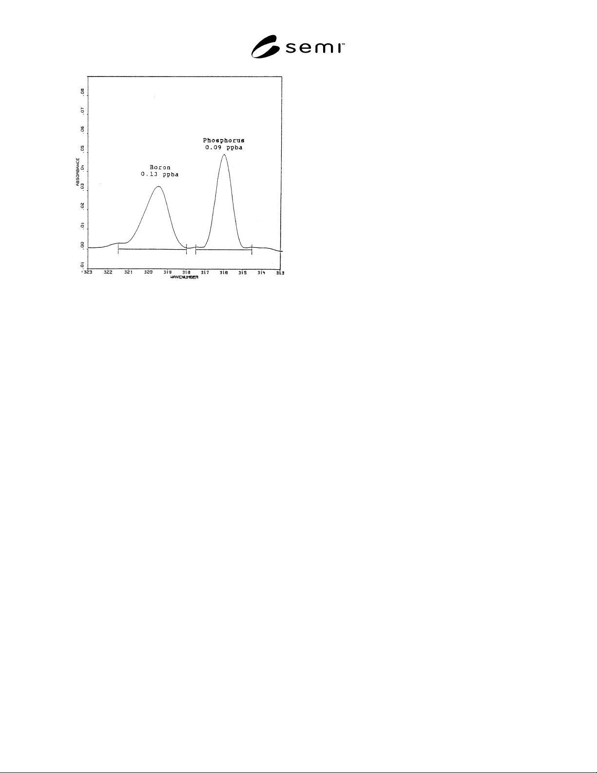
surrounding both peaks. Figures 2 and 3 show spectra
before and after, respectively, baseline correction for
boron and phosphorus spectral region.
12.1.2 Measure the area for the absorption peak
between the upper and lower wavenumbers given in
Table 1 for the integration limits. Most computer
algorithms handle this nicely. However, disable the
automatic zeroing of the baseline at the integration
limits. If not disabled, the integration would not
represent the baseline as established in Section 12.1.1
and may result in errors.
12.1.3 Repeat Sections 12.1.1 and 12.1.2 for each
component desired for each specimen measured.
SEMI MF1630-0704 © SEMI 2004 5
Table 1 Peak Location, Baseline and Integration Limits, and Calibration Factors
Baseline Limits Integration Limits
Element
Peak cm
−
1
Upper Lower Upper Lower
Factor
A
f(mm-cm)
Aluminum (Al) 473.2 479 467 475.2 471.2 32.7
Antimony (Sb) 293.6 296 289 295.1 292.1 10.6
Arsenic (As) 382.0 385 379 383.5 380.5 8.96
Boron (B) 319.6 323 313 321.5 318.0 9.02
Gallium (Ga) 548.0 552 544 549.5 546.5 42.4
Indium (In) 1175.9 1181 1169 1177.4 1174.4 244.0
Phosphorus (P) 316.0 323 313 317.5 314.5 4.93
A
The factors given here do not all have the same degree of certainty. The factors for boron, phosphorus, and arsenic are
believed to be correct to better than ± 10%. The other factors should be considered approximations and used for
estimations only. A discussion of the origin of these factors is given in Related Information 1.
13 Calculation
13.1 Calculate the concentration of each of the
electrically active impurity/dopant in each specimen
measured according to the following equation:
i
j
ij
ij
f
t
I
C = (1)
where:
C
ij
= concentration of impurity/dopant element i,
ppba, in sample specimen j,
I
ij
= integrated area of component i,
t
j
= thickness of sample specimen j, mm, and
f
i
= calibration factor for component i, mm-cm.
13.2 The concentration may be expressed as density in
units of atoms/cm
3
as follows:
ijij
CD
13
100.5 ×= (2)
Figure 2
Typical Infrared Spectrum in the Spectral Region
for Aluminum, Arsenic, Boron, and Phosphorus at
11 K
SEMI MF1630-0704 © SEMI 2004 6
Figure 3
Boron and Phosphorus Region Expanded and
Baseline Corrected
14 Report
14.1 Report the following information:
14.1.1 The instrument used, the operator, and the date
of the measurements,
14.1.2 Identification of specimens,
14.1.3 The results of the audit reference specimen on a
control chart or other suitable form,
14.2 For each sample specimen report the following
information:
14.2.1 The concentration of each impurity/dopant or the
detection limit if no peaks can be identified,
14.2.2 Sample thickness,
14.2.3 The FWHM for each absorption peak,
14.2.4 The apodization function used, and
14.2.5 The amount of zero-fills and resulting number of
data points/cm
−1
.
15 Precision
15.1 A within-laboratory precision was determined by
measurement of boron and phosphorus in a reference
specimen by multiple operators over a period of one
year. The relative precision was determined to be 8.5%
and 9.7% for boron and phosphorus, respectively, at
nominal concentrations of 0.095 and 0.072 ppba.
16 Bias
16.1 The bias of this test method is not known but
believed to be within ± 10% of an accepted reference
value.
17 Keywords
17.1 analysis of silicon; determination of dopants;
determination of impurities; electrically active
impurities; Fourier transform infrared; impurities;
silicon.