semi合集-English.pdf - 第6096页
SEMI G19-0997 © SE MI 1980, 1997 1 SEMI G19-0997 SPECIFIC A TI ON FOR DIP LEADFRAMES PRODUCED BY ETCHING 1 Preface This specification is a guideline for pro duction of DIP leadframes for plas tic molded semiconductor pac…

SEMI G18-96 © SEMI 1984, 19963
12.4 Any special packaging or shipping requirements
shall be agreed upon between supplier and purchaser at
the time of purchase.
13 Basis for Rejection
13.1 For the purposes of determining conformance
with the requirements prescribed in the specification,
any measured value outside the specified limiting
values shall be cause for rejection.
13.2 If objectionable material is found and rejected,
samples of the questionable material, with the defects
identified and marked, should be sent to the supplier
along with information as to order number, quantity
originally received, date received, and quantity rejected.
Rejected material should be held with adequate
protection and identification by the purchaser for a
reasonable amount of time, pending investigation by the
supplier.
NOTICE: These standards do not purport to address
safety issues, if any, associated with their use. It is the
responsibility of the user of these standards to establish
appropriate safety and health practices and determine
the applicability of regulatory limitations prior to use.
SEMI makes no warranties or representations as to the
suitability of the standards set forth herein for any
particular application. The determination of the
suitability of the standard is solely the responsibility of
the user. Users are cautioned to refer to manufacturer’s
instructions, product labels, product data sheets, and
other relevant literature respecting any materials
mentioned herein. These standards are subject to
change without notice.
The user’s attention is called to the possibility that
compliance with this standard may require use of
copyrighted material or of an invention covered by
patent rights. By publication of this standard, SEMI
takes no position respecting the validity of any patent
rights or copyrights asserted in connection with any
item mentioned in this standard. Users of this standard
are expressly advised that determination of any such
patent rights or copyrights, and the risk of infringement
of such rights, are entirely their own responsibility.
Copyright by SEMI® (Semiconductor Equipment and Materials
International), 3081 Zanker Road, San Jose, CA 95134. Reproduction o
f
the contents in whole or in part is forbidden without express written
consent of SEMI.
SEMI G19-0997 © SEMI 1980, 19971
SEMI G19-0997
SPECIFICATION FOR DIP LEADFRAMES PRODUCED BY ETCHING
1 Preface
This specification is a guideline for production of DIP
leadframes for plastic molded semiconductor packages
produced by the etching process. It is a design guideline
for packaging engineers, etchers, and mold
manufacturers and has been developed to meet the
requirements of automatic bonders.
2 Applicable Documents
2.1 SEMI Standards
SEMI G18 — Specification for Integrated Circuit
Leadframe Material Used in the Production of Etched
Leadframes
SEMI G10 — Standard Method for Mechanical
Measurement of Plastic Package Leadframes
2.2 Other Document
PCM1 D-300
1
— Standard Specification
3 Selected Definitions
burrs and protrusions — Fragments of excess material,
either horizontal or vertical, attached to the lead frame.
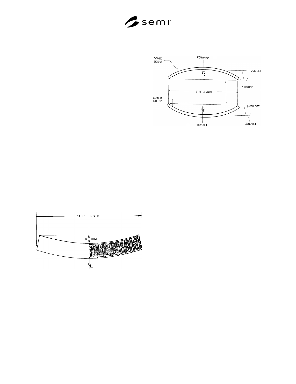
camber — Curvature of the leadframe strip edge (see
Figure 1).
Figure 1
Camber
coil set — Longitudinal bowing of the leadframe (see
Figure 2).
1 Photochemical Machining Institute, 4113 Barberry, Lafayette Hills,
PA 19444
Figure 2
Coil Set
compensation — Changes made in the dimensions on
the master artwork other than those specified on the
engineering artwork that allow for the process variables
(i.e., etch factor, undercut).
crossbow — Transverse bowing of the leadframe (see
Figure 3).
(enter graphic when available)
Figure 3
Crossbow
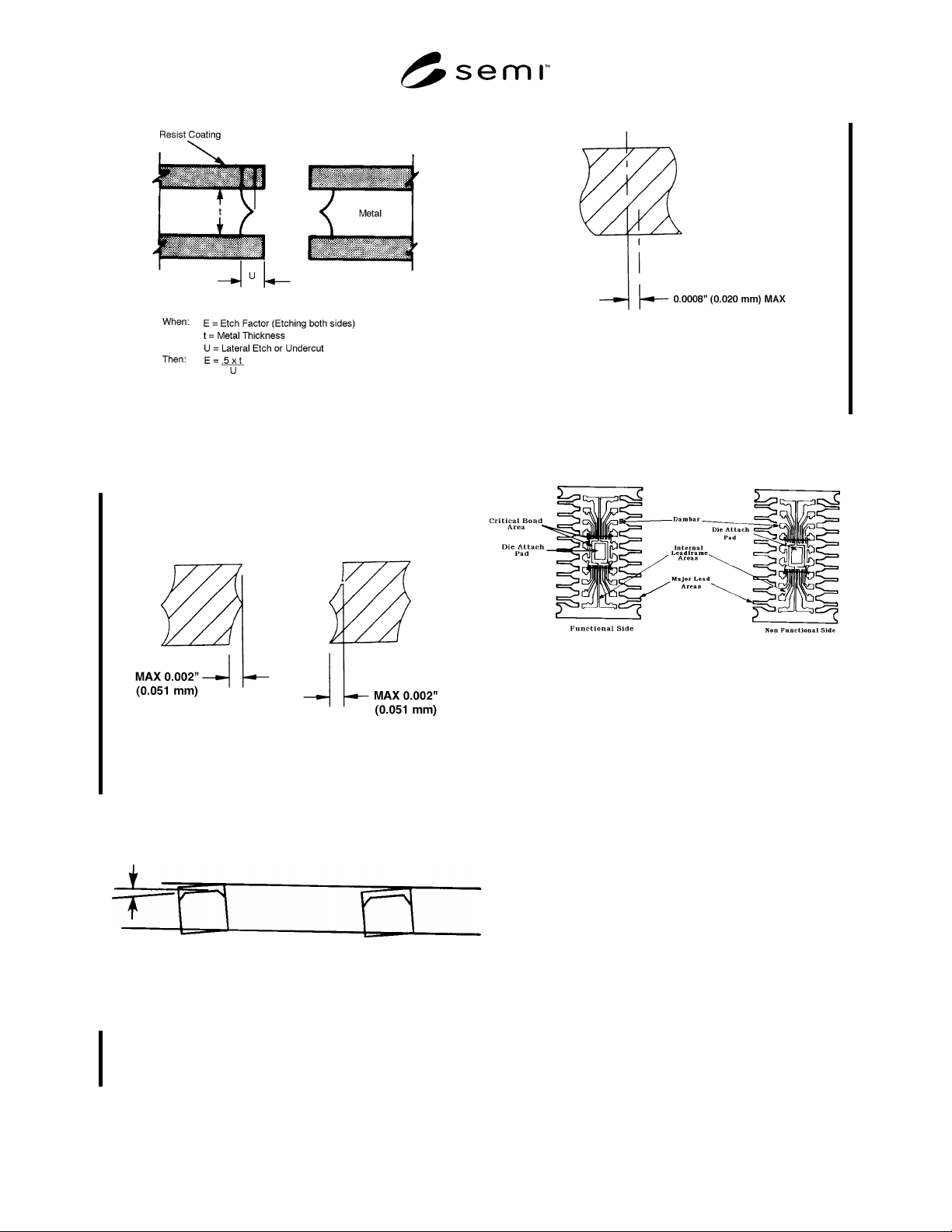
etch factor — The ratio of etched depth to the lateral
etch or undercut (see Figure 4).
SEMI G19-0997 © SEMI 1980, 1997 2
Figure 4
Undercut and Etch Factor
functional area — The die attach pad and wire bond
(lead tip) area.
lateral etch or undercut — The allowable bevelled edge
caused by the leadframe etchant attacking the metal
laterally as well as vertically (see Figure 5).
Figure 5
Overetching
lead twist — Angular rotation of the bond fingers (see
Figure 6).
Figure 6
Lead Twist
offset alignment accuracy — The top to bottom
alignment accuracy of the etched leadframe operation
(see Figure 7).
Figure 7
Etched Offset
pits — Shallow surface depressions or craters in the
leadframe material (see Figure 8).
Figure 8
Pits
resist breakdown — Etching under the edges of the
resist causing more than a standard undercut.
undercut — Bevelled edge caused by the etchant
attacking the metal laterally as well as vertically (see
Figure 4).
4 Ordering Information
Purchase orders for leadframes for plastic molded
semiconductor packages furnished to this specification
shall include the following items:
1. Drawing number and revision level
2. Material
3. Number of leads
4. Material certification
5. Number of units/strip
6. Plating requirements
7. Packaging and marking (see Section 8)